CS8803 OMSCS - GPU hardware and software notes
Content of these notes are from Georgia Tech OMSCS 7295 (Formally 8803): GPU Hardware and Software by Prof. Hyesoon Kim. They kindly allowed this to be shared publicly, please use them responsibly!
Module 1: Introduction of GPU
Objectives
- Describe the basic backgrounds of GPU
- Explain the basic concept of data parallel architectures
Readings
Required Readings:
- CUDA Programming guide, section 1-2, section 4
- Performance analysis and tuning for general purpose graphics processing units (GPGPU) (Chapter 1)
Optional Reading:
Module 1 Lesson 1: Instructor and Course Introduction
Course Learning Objectives:
- Describe how GPU architecture works and be able to optimize GPU programs
- Conduct GPU architecture or compiler research
- Explain the latest advancements in hardware accelerators
- Build a foundation for understanding the CUDA features (the course does not teach the latest CUDA features)
Course Prerequisites:
- Basic 5-stage CPU pipeline
- C++/Python Programming skill set
- Prior GPU programming experience is not necessary.
What is GPU?
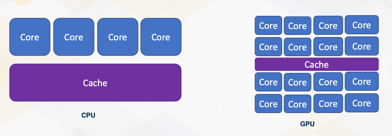
Have you ever wondered why GPUs are so relevant today? The answer can vary widely. While GPUs initially gained prominence in 3D graphics, they have since evolved into powerful parallel processors. Nowadays, GPUs are often associated with ML accelerators and high performance computing, showcasing their versatility. Let’s briefly compare CPUs and GPUs. One key distinction lies in their target applications. CPUs are tailored for single threaded applications aiming for maximum speed. In contrast, GPUs excel in parallelism, handling numerous threads simultaneously. CPUs prioritize precise exceptions, crucial for program correctness and debugging. On the other hand, GPUs focus on parallel computation and don’t prioritize precise exceptions as much. They leverage dedicated hardware for handling O/S and I/O operations, which naturally leads to that CPUs act as host and GPUs act as an accelerator.
GPU ISA
ISA refers to instruction set architecture.
Let’s touch on ISA. CPUs typically feature open ISAs, ensuring software compatibility across different hardware platforms. In contrast, GPUs operate in accelerator mode, with a driver translating code from one ISA to another for specific hardware. PTX was introduced to provide a public version of ISA, which is a virtual ISA.
| CPU | GPU | |
|---|---|---|
| Target applications | Latency sensitive applications | Throughput sensitive applications |
| Support precise exceptions? | Yes | No |
| Host-accelerator | Host | Accelerator |
| ISA | Public or open | Open/Closed |
| Programming model | SISD/SIMD | SPMD |
Additional information:
- SISD - Single Instruction, Single Data
- SIMD - Single Instruction, Multiple Data
- SPMD - Single Program, Multiple Data
SIMD (Single Instruction, Multiple Data):
- Imagine a group of chefs in a kitchen, all performing the same chopping motion (instruction) on different vegetables (data) at the same time. That’s SIMD!
- Strengths: Great for data-parallel tasks with repetitive operations on independent data elements. Think image processing, vector calculations, etc.
- Limitations: Requires data with consistent structure and can struggle with branching/conditional logic due to lockstep execution.
SPMD (Single Program, Multiple Data):
- Picture a team of artists, each working on a different section of the same painting (program) using their own techniques (data). That’s SPMD!
- Strengths: More flexible than SIMD, able to handle diverse tasks with branching and conditional logic. Often used for algorithms with complex workflows and distributed computing across multiple processors.
- Limitations: May have overhead due to thread management and communication needs.
Lastly, the program model for CPUs primarily centers around single threaded or single data operations while GPUs employ the single program multiple data model emphasizing parallelism.
Module 1 Lesson 2: Modern Processor Paradigms
Course Learning Objectives:
- Describe CPU design and techniques to improve the performance on CPUs
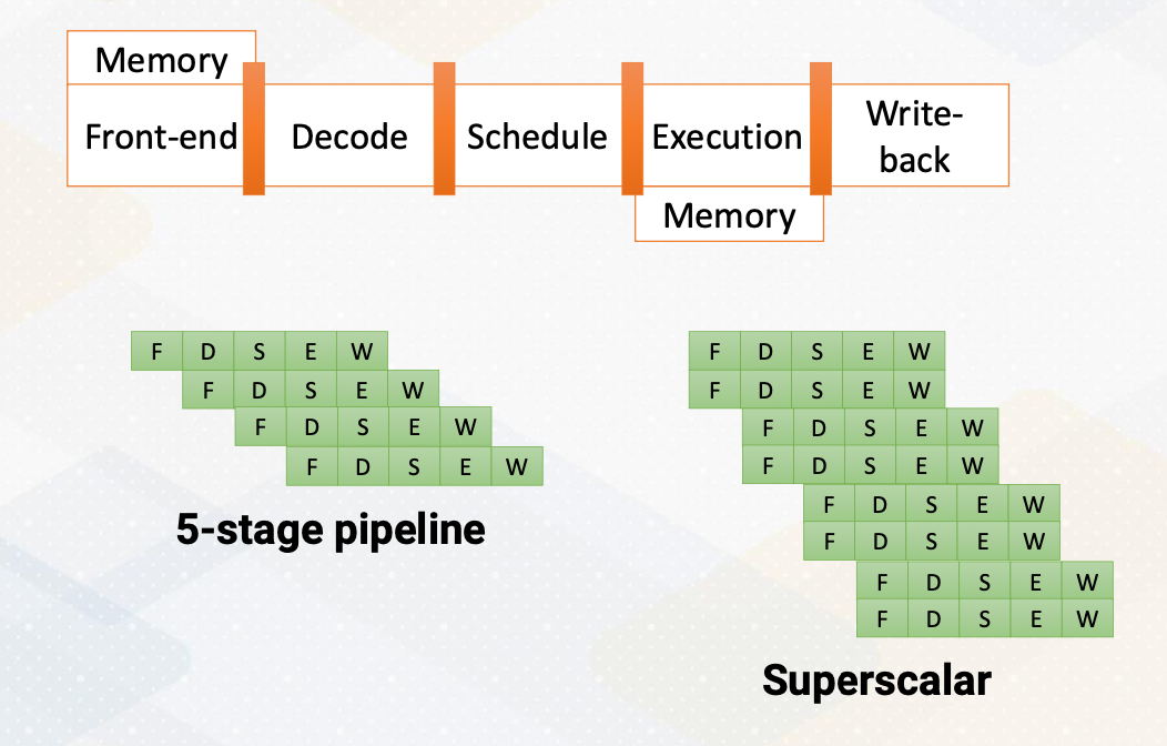
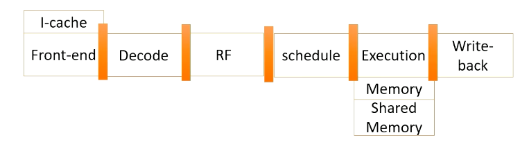
The foundation of CPU design consists of five stages; front-end, decode, rename, schedule, and execution.
- In the fetch stage, also called the front-end stage, instructions are fetched typically from an I-cache. In the decode stage, an instruction is decoded. In this stage, if this is an X86 instruction, a single instruction generates multiple micro uops.
- After instructions are decoded, typically registered files are accessed.
- The scheduler selects which instructions would be executed. In an in-order processor, the scheduler selects instructions based on the program order.
- For an out-of-order processor, it selects whichever ready to be excuted regardless of program order to find more ready instructions.
- The execution stage performs actual computation or also access the memory.
- In the write- back stage the result would be written back.
The above diagram illustrates the difference between a single issue processor versus superscalar processor. Superscalar processor enhances CPU performance by executing more than one instruction. They fetch, decode, and execute multiple instructions concurrently, effectively doubling performance.
Increasing Parallelism (1)
There are several ways of increasing execution parallelism. Superscalar processor increases the parallelism by handling more than one instruction, which essentially increases instruction level parallelism (ILP). ILP is crucial for CPU performance, but it determines how many instructions can run in parallel. Processors seek independent instructions to improve ILP and overall efficiency. In the superscalar processor, IPC instruction per cycle would be greater than one.
Instruction Level Parallelism
If a machine has two execution units, how many instructions can be executed simultaneously?
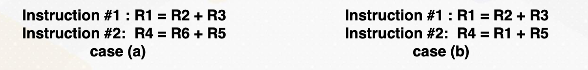
The slide shows two examples. In the first, two instructions are dependent, meaning they don’t rely on each other’s results. In this case, they can be executed concurrently, improving performance. In the second scenario, dependencies exist.
- Instructions are independent in case (a). Both instructions can be executed together.
- Instructions are dependent in case (b). Instruction #2 can be executed after instruction #1 is completed.
- Instruction level parallelism (ILP) represents parallelism.
- Out of order processor helps to improve ILP→find more independent instructions to be executed
- Improving ILP has been one of the main focuses in CPU designs.
Increasing CPU Performance
There are two main approaches. First, a deeper pipelines that increases a frequency, but it requires a better branch prediction. Second, CPUs have larger caches, which can reduce cache misses, thereby reducing memory access time significantly.
Increasing Parallelism (2)
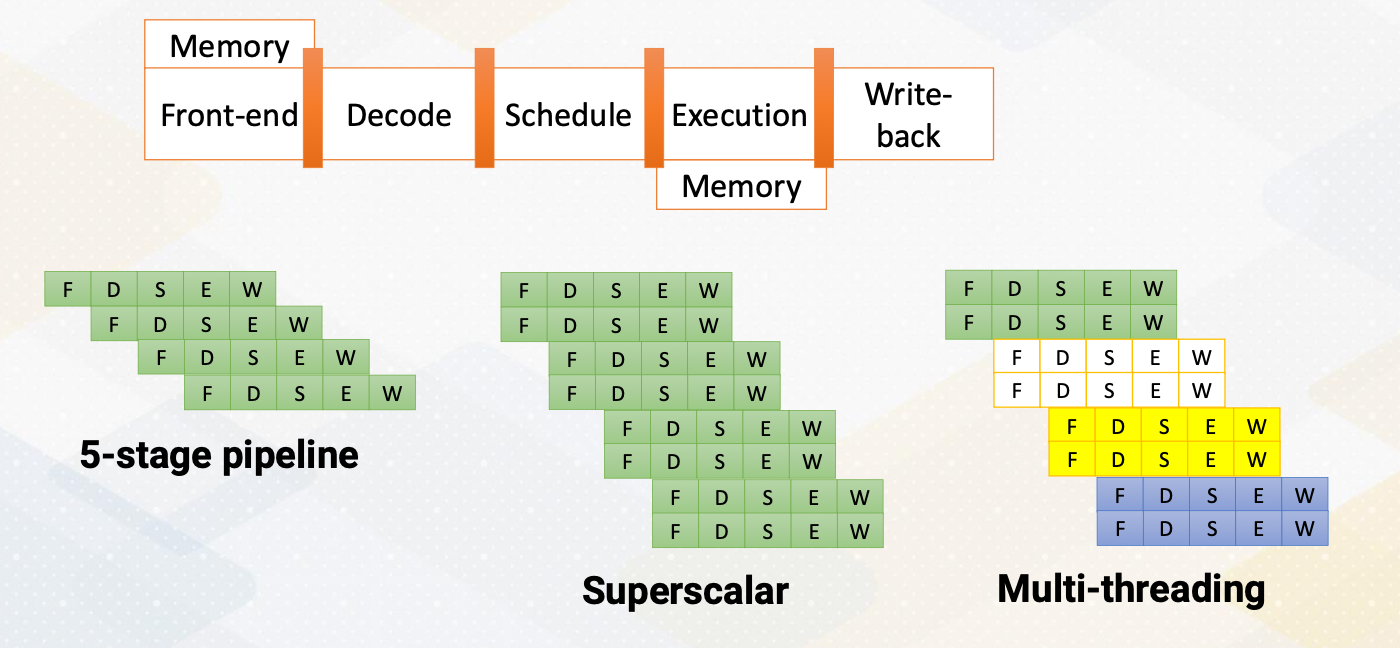
Another way of increasing parallelism is multi-threading. Multi-threading increase CPU performance by enabling multiple threads. By simply switching to another thread, it can examine more instructions that might be ready. Multi-threading is one of the key ingredients of high performance GPUs. Luckily, multi-threading does not require significant amount of hardware resource.
Multiprocessors
Multiprocessors are another powerful way of increasing performance. It has many processors by increasing the entire resource. Multiprocessor techniques are commonly used in both CPUs and GPUs. In this video, we explored how CPUs can enhance their performance by optimizing insuction level parallesm, increasing operating frequency, and scaling the number of cores in the system.
Module 1 Lesson 3: How to Write Parallel Programs
Course Learning Objectives:
- Describe different parallel programming paradigms
- Recognize Flynn’s classical taxonomy
- Explore a CUDA program example
Amdahl’s law
Let’s establish a fundamental concept in parallel programming known as Amdahl’s law. Imagine it as the processor, can execute parallel task and we have many parallel processors. We can quantify this performance boost using the formula:
\[\frac{1}{\frac{P}{N}+S}\]where P represents parallelism, S stands for the serial section, and the N is the number of processors involved.
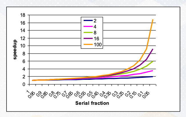
Visualizing this, we see that we have ample parallelism is available and the serial sections are minimal. Our performance gains scale almost linearly with the number of processors at play. However, when serial sections get significant, the performance scalability takes a hit. This underscores the critical importance of parallelizing applications with minimum serial sections and abundant parallelism. Even if you possess ample hardware resource, if a serial fraction exists, even 10%, it can impede your performance.
What to Consider for Parallel Programming
When we can parallelize the work, we can use parallel processors. But how do we write effective parallel programs?
- Increase parallelism by writing parallel programs
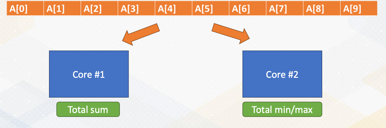
- Let’s think of an array addition and find min/max value
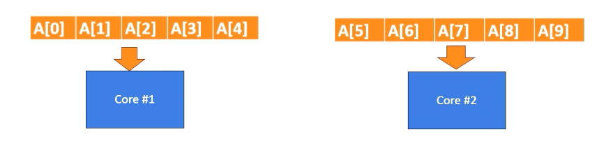
Task decomposition
- One core performs addition.
- The other core performs min/max operation
- Array [A] has to be sent to both cores.
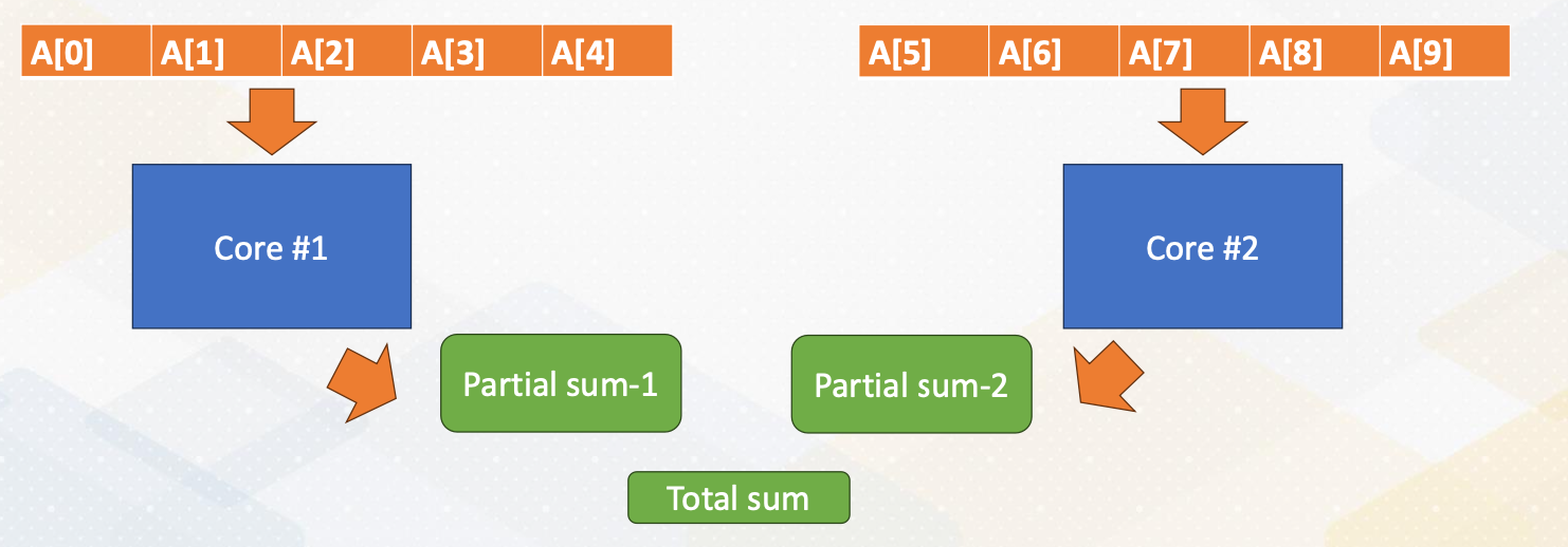
Data decomposition
- Split data into two cores
- Reduction operation is needed (both sum and min/max).
Flynn’s Classical Taxonomy
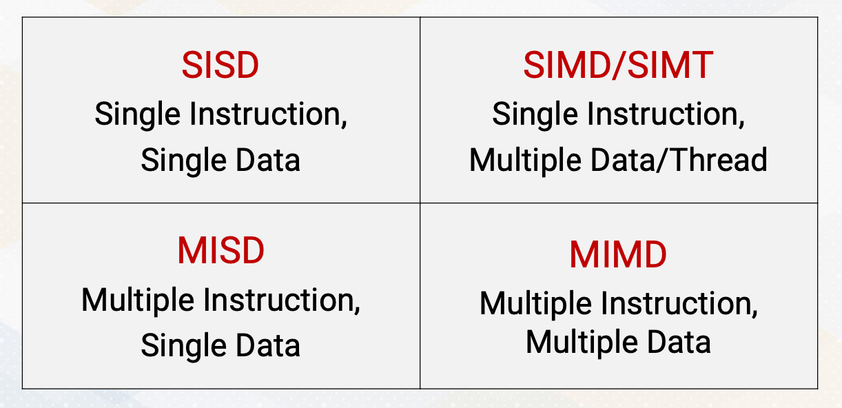
- SISD - Single Instruction, Single Data
- SIMD/SIMT - Single Instruction, Multiple Data / Thread
- MISD - Multiple Instruction, Single Data
- MIMD - Multiple instruction, Multiple Data
CPU Vs GPU:
- CPUs can be SISD, SIMD, and MIMD.
- And GPUs are typically SIMT.
The difference between SIMD and SIMT will be discussed later. Both fetches one instruction and operates multiple data. And CPU uses vector processing units for SIMD. And GPU have SIMT with many ALU (arithmetic logic unit) units.
Let’s look for another terminology, SPMD Programming, Single Program Multiple Data Programming. GPUs for instance favor SPMD, single program multiple data programming.
- All cores(threads) are performing the
same work(based on same program). But they are working ondifferent data. - Data decomposition is the typical programming pattern of
SPMD. -
SPMDis typical GPU programming pattern and the hardware’s execution model isSIMT. -
GPUprogramming uses SPMD programming style which utilizesSIMThardware.
To exemplify SPMD, let’s take a look at a CUDA program example. CUDA program has host and kernel. And here we’ll focus on the kernel code which runs on GPU device. The sum of array is also done by the following code. Each thread runs on the GPU, performing a specific task, which is adding its own value to the Array A. Thread IDs differentiate the task and all execute in parallel.
1
2
3

vector_sum() {
index ; // differentiate by thread ids
sum += A[index]; }
All cores(threads) are executing the same vector_sum().
Module 1 Lesson 4: Introduction to GPU Architecture
Course Learning Objectives:
- Gain a high-level understanding of GPU architecture
- Describe key terms including “streaming multiprocessors” and ”warp” and “wave-front”
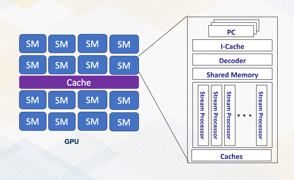
GPU Architecture Overview
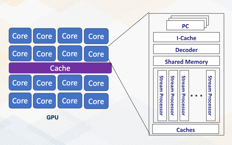
- Each core can execute multiple threads.
- CPU Cores are referred to as “ streaming multiprocessors (SM)” in NVIDIA term or SIMT multiprocessors
- Stream processors (SP) are ALU units, SIMT lane or cores on GPUs.
- In this course core ≠ stream processor
This slide shows an overview of GPU architecture. A GPU is composed of numerous cores, each can execute multiple threads. These cores work in harmony to handle complex task. The concept of CPU cores is more on streaming multiprocessor inside one SM you will find various components including an instruction cache decoder, shared memory, and multiple execution units referred to as stream processors in GPU terminology. These stream processors are essentially one SIMT lane or ALU and it is called cores on GPUs. To reduce the confusion between CPU cores and GPU cores in this course we will not refer SIMT lane as a core.
GPU Pipeline
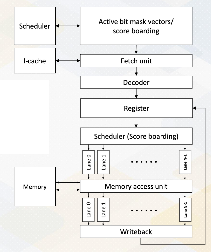
This slide shows a GPU pipeline.
- This stage include the fetch stage
- where each work item is fetched and
- multiple pieces registers are used to support multi threaded architectures.
- These are various schedulers such as the round-robin scheduler
- or the more sophisticated greedy scheduler which selects task based on the factors like cache miss or branch predictions.
- The decode stage processes, the fetched instructions, and
- the register values are read.
- Schedulers or score boarding select ready warps.
- Those selected warps would be executed by execution unit and
- then the result would be written back.
Execution Unit: Warp/Wave-front
In this course warp and the wavefront would be used interchangeably.
Multiple threads are forming what’s known as a warp or wave-front which is a fundamental unit of execution and consists of multiple thread. A single instruction is fetched per warp and multiple threads will be executed. In the world of micro architecture, the term warp size is pivotal. It has remained constant at 32 for an extended period but this can be changed in future.
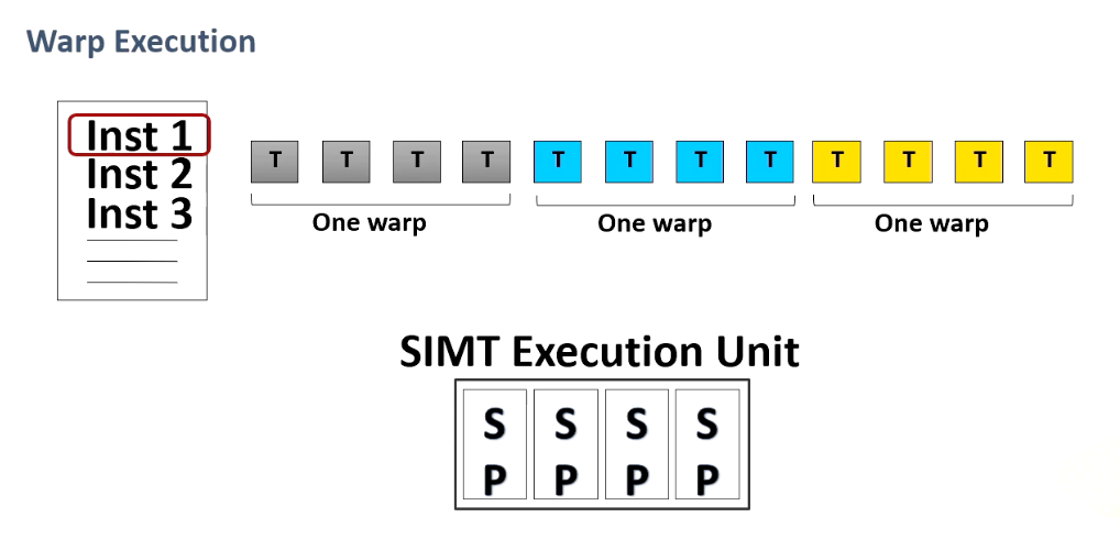
This diagram illustrates a warp execution. Here is a program which has multiple instructions and programmer specifies a number of threads for a kernel and we have SIMT execution unit and threads are grouped as a warp.
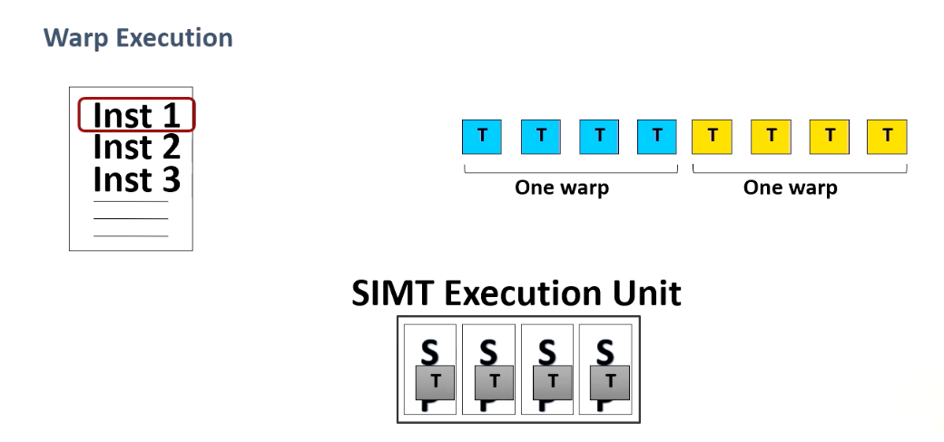
For a given instruction when source operands are ready the entire warp will be executed. When another warp is ready, this will be executed , and another one. So programmers specify 12 threads and in this example the warp size is four threads. And the entire four threads are executed one at a time.
Module 1 Lesson 5: History Trend of GPU Architechtures
Course Learning Objectives:
- Describe the evolution history of GPUs
- Describe the evolution of traditional 3D graphics pipelines
Traditional 3D Graphics Pipeline
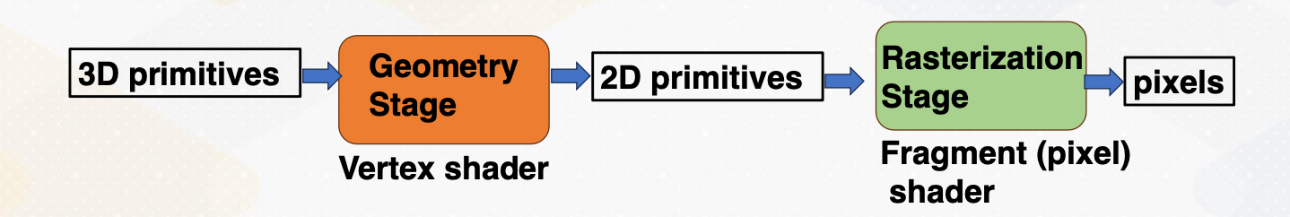
- Traditional pipelined GPUs: separate Vortex processing and pixel processing units
- Programmable GPUs: introduction of programmable units for vertex/pixel shader
- Vertex/pixel shader progression to CUDA programmable cores (GPGPU)
- Modern GPUs: addition of ML accelerator components (e.g., tensor cores), programmable features.
Let’s look at a traditional 3D graphics pipeline. In the early days, GPUs were born from the 3D graphics tradition where their primary role was to proceed 3D primitives provide as input. These primitives underwent various stages, including geometry processing, eventually generating in the creation of 2D primitives, which were then rendered into pixel on your screen.
This pipeline formed the core of early GPU architectures. As GPUs evolved, so did their capabilities. The shaders, which were initially fixed function units, gradually became more programmable. This transformation paved the way for unified shader architectures, a hallmark of the Tesla architecture. With this innovation, GPUs became versatile tools capable of handling both graphics and general purpose computing tasks.
The era of GPGPU programming had begun. GPGPU term was used to differentiate, to use GPU for general purpose computing. Nowadays, GPU are more widely used for other than 3D graphics. So this differentiation is not necessary. With each iteration of GPUs extended their capabilities further, Vertex and pixel shader gave way to more powerful cores such as tensor cores, aimed at accelerating tasks beyond traditional graphics processing. The application space for GPUs expanded dramatically, encompassing tasks like machine learning acceleration and more.
Programmable GPU Architecture Evolution
-
Cachehierarchies (L1, L2 etc.) - Extend FP 32 bits to
FP 64bits to support HPC applications - Integration of
atomicandfast integer operationsto support more diverse workloads - Utilization of
HBMmemory (High bandwidth memory) - Addition of smaller floating points formats (
FP16) to support ML workloads - Incorporation of
tensor coresto support ML workloads - Integration of
transformer coresto support transformer ML workloads
Programmable GPU architectures have evolved in various directions. First, it introduces L1 and L2 caches. It also increased the precision of polluting point from single precision 32 bit to double precision 64 bit to accommodate more high performance computing applications. It also introduces atomic and fast integer operations to support more diverse workloads.
The introduction of high bandwidth memory, HBM, marked another significant milestone. HBM integrate into the GPU’s memory subsystem offered unprecedented data transfer rates. GPUs leveraged this cutting edge technology to meet the demands of modern workload. To increase ML computation parallelism, it also supports a smaller floating point format such as FP16. It also adopts tensor core and transformer core to support ML applications.
NVIDIA H100
Let’s look at 2023’s latest NVIDIA GPU architecture which is H100.
- They support various precisions, FP32, FP64, FP16, Integer 8 and FP8 formats.
- It also has tensor cores similar to previous generation of GPUs, and
- introduced new transformer engine, ML cores, GPU cores, and tensor cores play pivotal roles in meeting the demands of modern ML applications.
- Increased capacity of large register files
- Concepts like tensor memory accelerator promise even greater capabilities.
- Furthermore, the number of stream multiprocessor (SMs) and the number of floating point (FP) units keep increasing to provide more compute capability.
- On top of that, it uses NVIDIA NVLink switch system to connect multiple GPUs to increase parallelism even more.
Module 2: Parallel Programming
Objectives
- Describe the basic backgrounds of GPU
- Explain the basic concept of data parallel architectures
Readings
Required Reading:
Optional Reading:
Module 2 Lesson 1: Parallel Programming Patterns
Course Learning Objectives:
- Provide an overview of different parallel programming paradigms
How to Create a Parallel Application
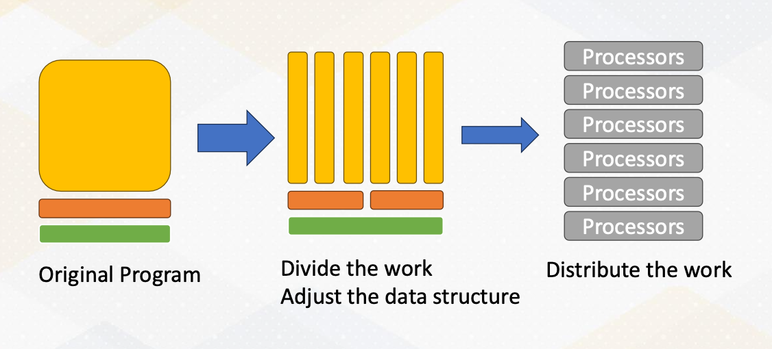
The original program has many tasks. We divide the work and adjust the data structure to execute the task in parallel. Then we dispute the work to multiple processors
Steps to Write Parallel Programming
- Step 1, discover concurrency.
- The first step is to find the concurrency within your problem. This means identifying opportunities for parallelism in your task or problem. This is often the starting point for any parallel programming.
- Step 2, structuring the algorithm.
- Once you’ve identified the concurrency, the next step is to structure your algorithm in a way that can effectively exploit this parallelism. Organizing your code is key to harnessing the power of parallelism.
- Step 3, implementation.
- After structuring your algorithm, it’s time to implement it in a suitable programming environment. In this step, you choose which program language and tools to use.
- Step 4, execution and optimization.
- With your code written, it’s time to execute it on a parallel system. During this phase, you will also focus on fine- tuning the code to achieve the best possible performance.
Parallel Programming Patterns
There are five popular parallel programming patterns:
- Master/Worker Pattern
- SPMD Pattern (Single Program, Multiple Data)
- Loop Parallelism Pattern
- Fork/Join Pattern
- Pipeline Pattern
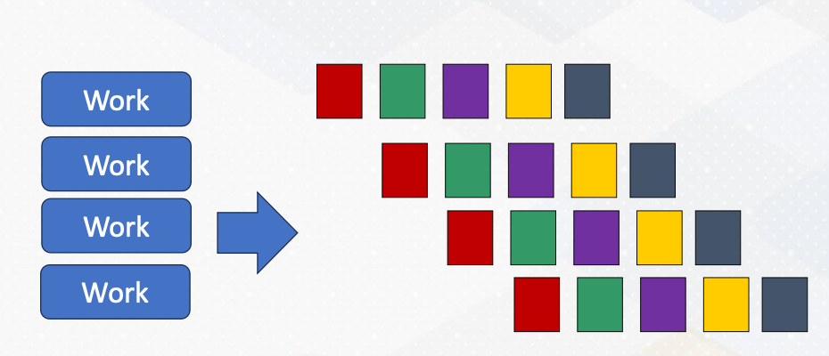
Master/Worker Pattern
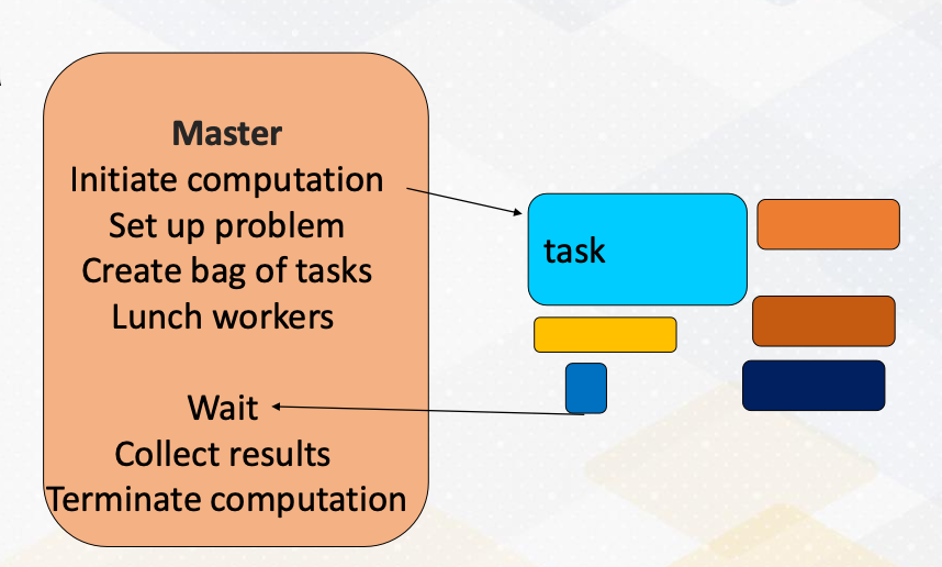
First of all, we have the master worker pattern. It is single program and multiple data. There is a master process or thread which manages a pool of worker process/threads, and also a task queue. In this figure, orange box represents master threads.
Then there are many workers and they execute tasks concurrently by dequeuing them from the shared task queue.
In this figure, different color boxes show worker threads who execute different tasks. This master/worker pattern is particularly useful for the task that can be broken down into smaller independent pieces.
Loop Parallelism PAttern
1
2

for (i = 0; i < 16; i++)
  c[i] = A[i]+B[I];
Next, loop parallelism pattern. Loops are a common and excellent candidate for parallelism. What makes them appealing for parallel programming is that many loops involve repetitive independent iterations. This means that each iteration can be executed in parallel. Another note is that unlike master/work pattern, tasks inside the loops are typically the same.
SPMD Pattern
Single program, multiple data
Now let’s talk about SPMD programming pattern. SPMD stands for single program multiple data. In this approach, all processing elements execute the same program in parallel, but each has its own set of data. This is a popular choice, especially in GPU programming.
Fork/Join Pattern
The fourth paradigm is the fork/join pattern. Fork/join combines both serial and parallel processing. Parent task create a new task which is called fork, then wait for their completion which is called join before continuing with the next task. This pattern is often used in programming with a single entry point.
Pipeline Pattern
Finally, let’s explore the pipeline pattern. The pipeline pattern resembles a CPU pipeline where each parallel processor works on different stages of a task. It’s an ideal choice for processing data streams. Examples include: signal processing, graphics pipelines, and compression workflows, which consist of decompression, work, and compression.
This animation illustrates a pipeline programming pattern. Each color represents different pipeline stages. Data work is coming continuously, and by operating different work, it provides parallelism.
Module 2 Lesson 2: Open MP vs. MPI (Part 1)
Explore shared memory programming, distributed memory programming, and take a closer look at the world of OpenMP.
Course Learning Objectives:
- Explain the fundamental concepts of shared memory programming
- Describe key concepts essential for shared memory programming
- Explore the primary components of OpenMP programming
Programming with Shared Memory
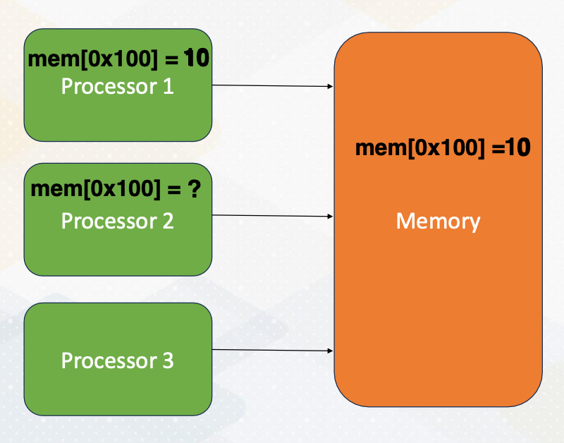
Let’s start by understanding shared memory programming, a core concept in parallel computing. In shared memory systems, all processors can access the same memory. The following animation illustrates the steps. First, processor 1 updates a value, then processor 2 can observe the updates made by processor 1, by simply reading values from the shared memory.
Programming with Distributed Memory
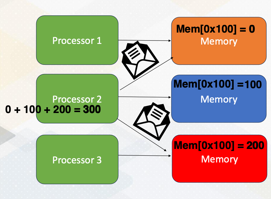
Now let’s just switch gears and explore programming with distributed memory. Unlike a shared memory system, in distributed memory systems, each processor has its own memory space. To access data in other memory space, processors send messages as the following. The same memory address is located in three different memory systems. Processor 2 requests messages from processor 1 and processor 3. Each processor sends data 0 from processor 1, and 200 from processor 3. The updated data are sent by messages, then the processor performs additions using the updated value. Then the updated value will be written back to the memory.
Overview of Open MP
Before we dive deeper into shared and distributed memory, let’s get an overview of OpenMP. OpenMP is open standard for parallel programming on shared memory processing system.
OpenMP is a collection of compiler directives, library routines, and environment variables to write parallel programs.
Key Tasks for Parallel Programming
Here are the key tasks for parallel programming:
- parallelization,
- specifying threads count,
- scheduling,
- data sharing,
- and synchronization.
What is Thread?
We’ll go over these concepts. First, let me provide a little bit of background on thread, which plays a pivotal role in parallel computing. What is thread? Thread is an entity that runs on a sequence of instructions.
Another important fact to know is that a thread has its own register and stack memory. So is thread equivalent to core? No, thread is a software concept. One CPU core could run multiple threads or just a single thread. Please also note that the meaning of thread is different on CPUs and GPUs.
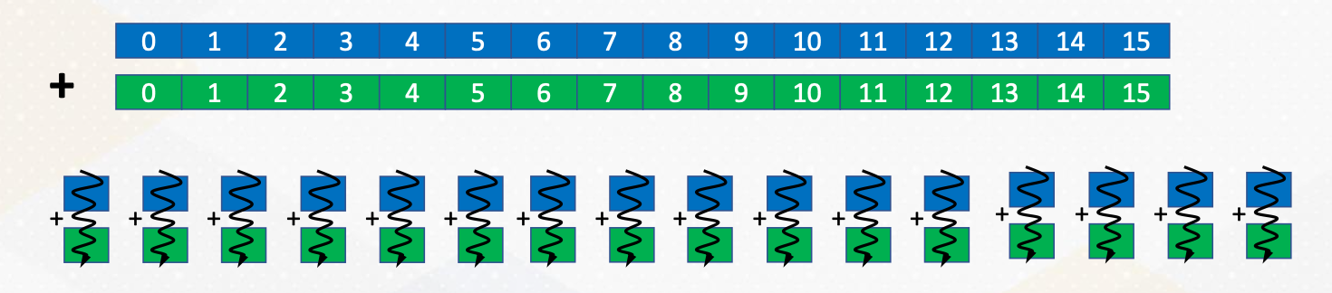
Review: Data decomposition
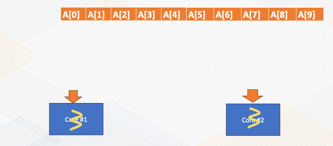
Let’s review data decomposition, which we saw in Module 1. Let’s decide we want to use data decomposition method. Here we have a 10 element array. An array is split into two cores.
The half of the data is sent to core 1, and the remaining half of the data is send to core 2 and they will be executed in parallel. In practice, modern CPUs can execute multiple threads within one core. However, for simplicity, we assume that one core executes one thread in this illustration.
Example: Vector sum
1
2
3
4
5
6
7
8
9

int main() {
  const int size = 10; // Size of the array int data[size];
  int sum = 0;
  for (int i = 0; i < size; ++i) {
    sum += data[i];
    }
  std::cout << "Sum of array elements: " << sum << std::endl;
  return 0;
  }
Here is a serial version of vector sum code. We have a for loop which iterates from 0 to 10 and then computes the sum of the elements.
Manual Parallelization processes
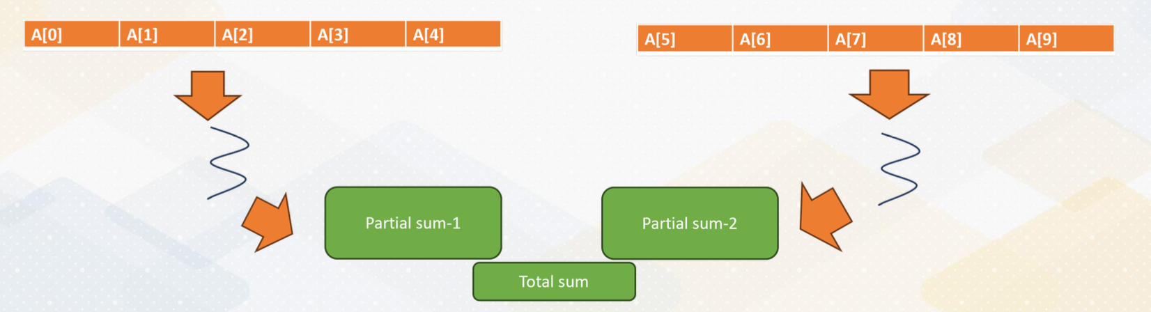
This slide shows the actual parallelization steps. In the first step, we create two threads. In the second step, we split the array into two and give a half array to each thread. In the third step, we merge two partial sums. One of the challenges is how to merge values by two threads. This merge is one of the reduction operations.
Reduction Operation in Shared Memory
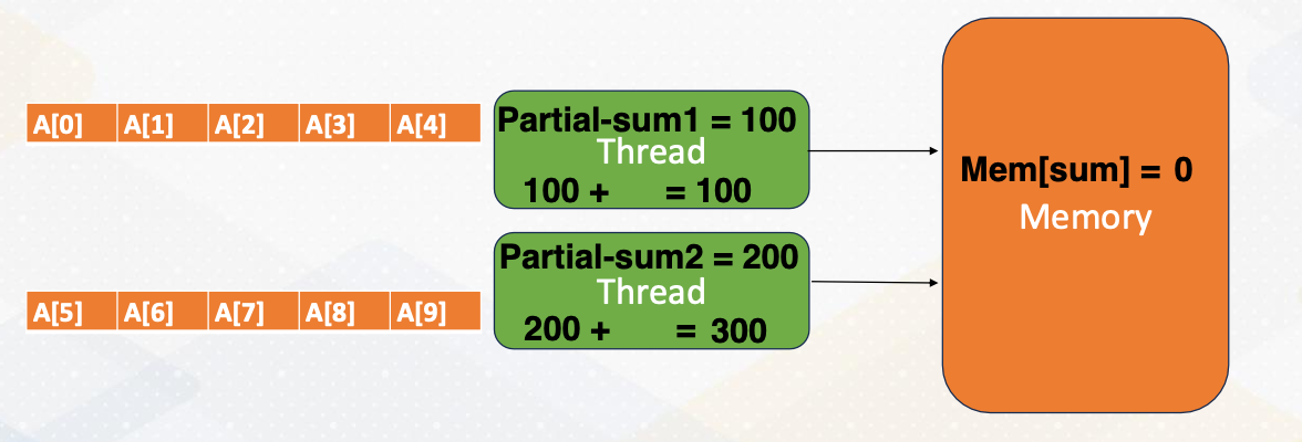
Let’s look at reduction operation in shared memory in detail. First, each thread computes partial sum. The one thread updates the total sum value in one memory. The memory gets updated. The other thread reads updated value from the memory, and then adds the partial sum into the total sum and updates total value in the memory. In this process, we need to make sure only one thread updates the total sum in the memory that can be handled by Mutex.
Mutex Operation
What is Mutex? Mutex, mutual exclusion ensures only one thread can access a critical section of code at a time.
- What if both threads try to update the total sum.
- In previous example Some would be either 100, or 200 instead of 300.
- We need to prevent both threads from updating the total sum variable in the memory because the sum variable is a
shared data. - Updating shared variable is
critical section of code. - Mutex ensures only one thread can access critical section of code. First, we use a lock, which is acquiring a Mutex to enter the critical section.
- After completing a critical section, it unlocks which is releasing a mutex so others are allowed to access the critical section.
Low Level Programming for Vector Sum
If we do this work using low level programming such as p-thread, it requires manual handling of thread creation, joining and Mutex operations.
Vector Sum in OpenMP
1
2
3
4
5
6
7
8
9
10
11
12
13

#include <iostream>
#include <omp.h>
int main() {
  const int size = 1000; // Size of the array int data[size];
  // Initialize the array
  int sum = 0;
  # pragma omp parallel for reduction(+:sum)
  for (int i = 0; i < size; ++i) {
    sum += data[i];
  }
  std::cout << "Sum of array elements: " << sum << std::endl;
  return 0;
}
Luckily, this step can be simplified by using OpenMP APIs. All we need to do is adding pragma omp parallel for reduction +sum. Parallel for invokes loop parallelism in pattern. It generates multiple threads automatically.
pragma omp parallel for reduction(+:sum)
What is reduction + sum?
- It is a compiler directive which is the primary construct.
- It works for C/C++, or Fortran which is used widely in HPC applications.
- Compiler replaces directives with calls to runtime library.
- Library function handles thread, create/join.
- The semantics are
#pragma omp directive [ clause [ clause ] ... ].- Directives are the main OpenMP construct. For example,
pragma omp parallelfor Clause provides additional information such asreduction (+:sum)
- Directives are the main OpenMP construct. For example,
- Reduction is commonly used, so it has a special reduction operation.
Module 2 Lesson 3: Open MP vs. MPI (Part 2)
We will describe key components of both OpenMP and MPI programming.
Course Learning Objectives:
- Extend your understanding of the concept of scheduling in OpenMP
- Describe key components of OpenMP and MPI programming
How many Threads?
The following for loop will be executed in parallel by the number of threads. Then the question is, can you control this number?
1
2
3
4

#pragma omp parallel for reduction(+:sum)
for (int i = 0; i < size; ++i) {
  sum += data[i];
}
The answer is yes. You can specify the number of threads using the environment variable, OMP_NUM_THREADS By default, this number is the same as the hardware parallelism, such as the number of cores. Alternatively, you can use the omp_set_num_threads() function to define the number of threads directly within your code.
Scheduling
Now, let’s tackle another important concept of a scheduling within parallel programming. Imagine a scenario where you have a vector of one million elements and you want to distribute this work among five threads, but you only have two cores. How do you ensure each thread makes progress evenly?
We probably want to give 200k elements to each thread. This works well if each thread can make the same progress. But what if each thread makes a different progress? Why would this happen? Because we have allocated a total of five threads. Here is the interesting part. One core has three threads while the other core has only two threads.
As a result, the three threads on one core would have significantly fewer resources compared to the case where each core has an equal number of threads.
Static Scheduling/Dynamic Scheduling
To address the challenges of uneven progress among thread, we have various scheduling options.
- Option 1 (static scheduling): still give 200K elements to each thread
- in the first option known as static scheduling, we continue to allocate a consistent chunk of work to each thread. We will give 200k elements to each thread. This approach assumes that each thread will make roughly the same progress.
- Option 2 (dynamic scheduling): give 1 element to each thread and ask it to come back for more work when the work is done
- this option takes a different approach. In this scenario, we give just one element to each thread initially and allow them to come back for more work when they finish processing their assigned element. This dynamic nature allows threads to request additional work as needed, ensuring efficient resource utilization. This is called dynamic scheduling.
- Option 3 (dynamic scheduling): give 1000 elements to each of them and ask it to come back for more work when the work is done
- asking more work for every element becomes too expensive. So in the third option, we initially allocate larger chunks of work saying 1,000 elements to each thread. As with Option 2, threads can return for more work once they complete their assigned portion. This approach aims to strike a balance between granularity and efficiency.
- Option 4 (guided scheduling - chunk size varies over time): initially give 1000, but later start to give only 100 etc.
- lastly, we have a guided scheduling where we start with the larger chunk sizes such as 1,000 elements, but progressively decrease the chunk size over time. This approach adapts to the run time conditions, ensuring that threads with varying progress rates can efficiently utilize resources. For example, if some threads finish faster, they receive larger chunks, while slow threads get smaller chunks.
Giving one element or 1,000 elements refers to different chunk sizes. And in guided scheduling, which is option 4, chunk size varies over time. Each of these scheduling options offer distinct advantages and trade-offs. The choice depends on the specific workload and the dynamic nature of the threads progress. By selecting the most suitable scheduling option, we can optimize resource utilization and overall program efficiency. Dynamic scheduling can adopt run time effect (maybe some threads got scheduled to an old machine etc.)
Data Sharing
Now let’s shift our focus to data sharing, an essential consideration in parallel programming. Data sharing involves distinguishing between private and shared data. While partial sums are private data. The overall sum is shared among thread. And it’s crucial for programmers to specify data sharing policies.
Thread Synchronization
Thread synchronization is another critical aspect of parallel programming. It ensures correct execution. Barrier, critical section and atomics are examples of thread synchronization.
Barrier
A common synchronization construct is the barrier which is denoted by #pragma omp barrier. It ensures that all participating threads reach a specific synchronization point before proceeding. This is crucial for tasks like that have dependencies between tasks such as sorting and update.
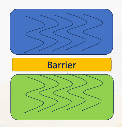
- Synchronization point that all participating threads reach a point
- Green work won’t be started until all blue work is over.
Critical Section
1
2

#pragma omp critical [(name)]
  // Critical section code
Critical section should only be updated by one thread at a time. They play a vital role in preventing data race conditions. For example, incrementing a counter. This can be done by denoting #pragma omp critical [(name)].
1
2
3
4
5

#pragma omp parallel num_threads(4) {
  #pragma omp critical {
      //critical section code
  }
}
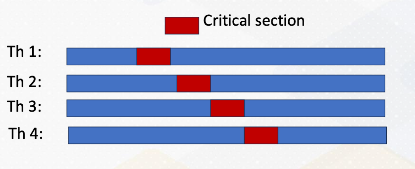
As the following code example shows, critical section code is guarded by pragma omp critical directives. Even though there are four threads, only one thread would enter the critical section as illustrated in the above diagram. The red color represent critical section and only one thread enters the critical section. We have already studied mutex to perform this type of critical sections.
Atomic
Let’s explore atomic operations in OpenMP, denoted by #pragma omp atomic.
These operations guarantee that specific tasks are performed atomically. Meaning that they either complete entirely or not at all. For instance, consider incrementing a counter. Here is a code example.
1
2
3
4
5

#pragma omp parallel for
for (int i = 0; i < num_iterations; ++i) {
  #pragma omp atomic counter++;
  // Increment counter atomically
}
Counter value is incremented with atomic. Incrementing a counter requires loading the counter value, adding and storing, which are three different operations. Atomic operations ensure that all these three operations will happen altogether or none of them. Thereby, counter value is incremented by only one thread at once. These operations are vital for safeguarding data integrity and avoiding data race conditions. They can be implemented using Mutex or hardware support, depending on the specific scenario.
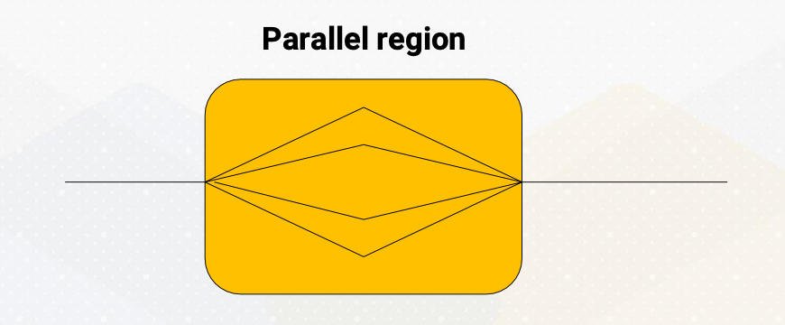
Parallel Sections
Sometimes work needs to be done in parallel, but not within a loop. How can we express them?
1
2
3
4
5
6
7
8
9
10
11

#pragma omp parallel sections
{
  #pragma omp section
  {
  // work-1
  }
  #pragma omp section
  {
  // work-2
  }
}
To address this, openMP provides the section directives. The code shows an example. Work 1 and work 2 will be executed in parallel. This directive can be combined with other constructions ordered or single. Work specified within sections can be executed in parallel. They are very useful with various programming patterns.
Example of Parallel Sections: Ordered
1
2
3
4
5
6
7
8
9
10
11

#pragma omp parallel
{
  #pragma omp for ordered
  for (int i = 0; i < 5; i++) {
    #pragma omp ordered
    {
      // This block of code will be executed in order
      printf("Hello thread %d is doing iteration %d\n", omp_get_thread_num(), i);
      }
    }
  }
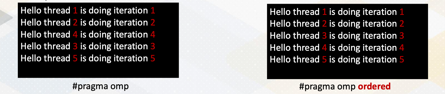
Here is an example demonstrating the orderered construct within parallel sections. It ensures that threads are executed as an ascending order in the left side without ordered construct, threads are executed out of order. In the right side with ordered construct, threads are printing messages in order.
Example of Parallel Sections: Single
1
2
3
4
5
6
7
8
9

#pragma omp parallel
{
  #pragma omp single
  {
    // This block of code will be executed by only one thread
    printf("This is a single thread task.\n");
  }
  // Other parallel work...
}
Similarly, the single construct within parallel sections ensures that only one thread executes the specified task (no exception about which thread will do). It’s useful for scenarios where no specific thread is expected to perform the work by only one thread. This can be used for different tasks such as initialization. So in this example, we see only one single printf message.
Module 2 Lesson 4: Programming with MPI
Course Learning Objectives:
- Describe fundamental concepts of distributed memory parallel programming
- Gain understanding of MPI (Message Passing Interface) programming
Why Study OpenMP and MPI?
You might be wondering, why do we need to study OpenMP and MPI. Well, the answer lies in the complexity of GPU programming. CUDA programming combines elements of shared memory and distributed memory programming. Some memory regions are shared among all cores, while others remain invisible and need explicit communications.
MPI Programming
Now let’s dive into MPI programming. MPI, or Message Passing Interface, is a powerful communication model for parallel computing. It allows processes to exchange data seamlessly.
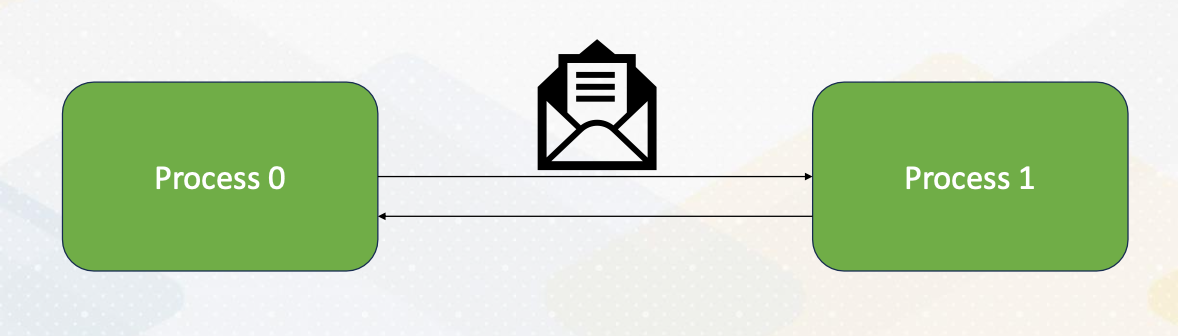
Here the diagram illustrates that Process 0 sends an integer value to Process 1 using MPI_send() And Process 1 receives the value sent by Process 0 using MPI_recv().
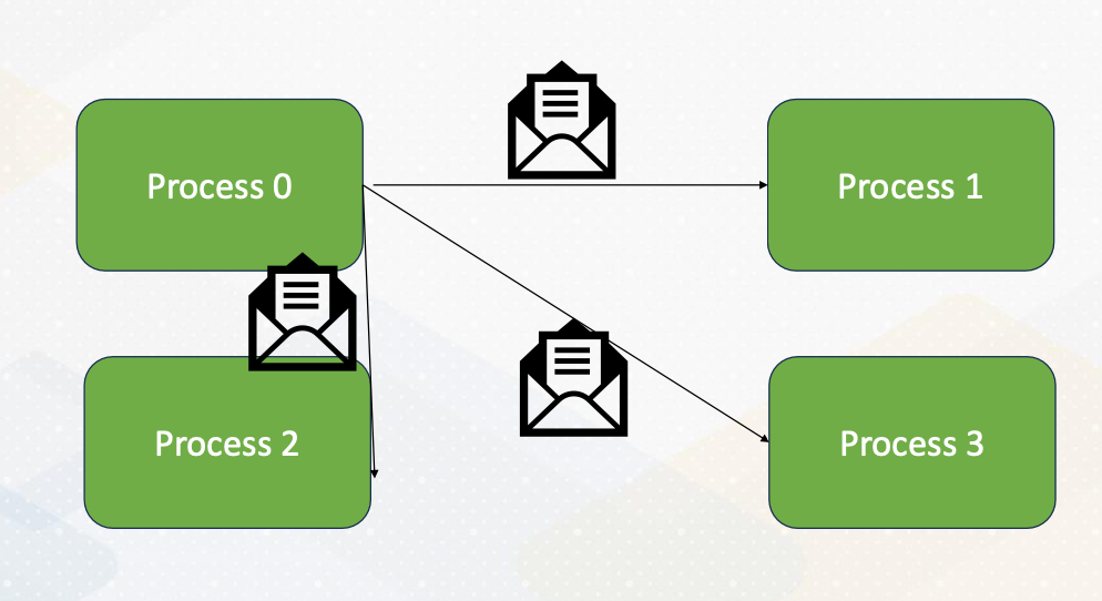
Broadcasting
MPI provides various communication functions, and one of them is MPI_Bcast() or broadcast. This function allows you to broadcast data from one process to all other processes in a collective communication manner. It’s a valuable tool for sharing information globally.
Stencil Operations
To give a more explicit example of message passing, here we take a look at stencil operations, which is common in HPC, High-Performance Computing.
This involves computations with the neighborhood data. For example, in this diagram, computing c is the average of 4 neighborhood, and we want to apply this operation to all elements in a dataset.
Stencil Operations (cont’d)
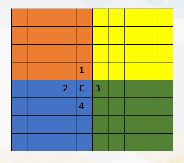
Let’s assume that:
- we want to compute the stencil operation with the four processes in the distributed memory systems.
- It’s important to note that in MPI, each process can access only its own memory regions.
- But what happens when you need to compute C, which requires access to data in other memory regions? This is where the challenge arises. (For example C where it requires numbers from orange and green area)
Communicating Boundary Information
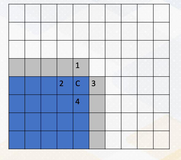
To overcome the challenge of computing C, we need to communicate boundary information, which is the gray color in this diagram. This means sending data from one process to another using messages. It’s a crucial aspect of MPI programming, especially in scenarios where data dependencies span across processes.
Module 3: GPU Programming Introduction
Objectives
- Describe GPU programming basic
- Be able to program using CUDA
Readings
Module 3 Lesson 1: Introduction of CUDA Programming
Course Learning Objectives:
- Write kernel code for Vector Addition
- Explain basic CUDA programming terminologies
- Explain Vector addition CUDA code example
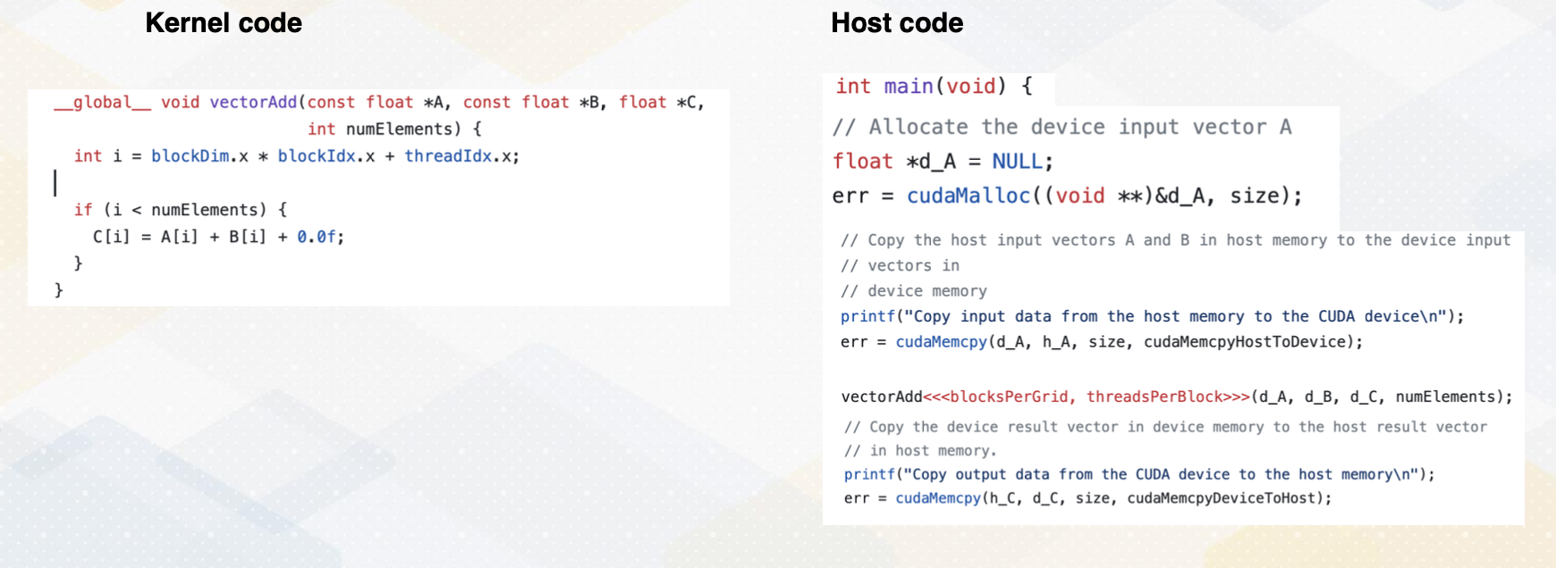
Cuda Code Example: Vector Addition
Kernel code
1
2
3
4
5
6
7

__global void vectorAdd(const float *A, const float *B, float *C, int numElements){
  int i = blockDim.x * blockIdx.x + threadIdx.x;

  if (i < numElements){
    C[i] = A[i] + B[i] + 0.0f
  }
}
Host Code
1
2
3
4
5
6
7
8
9
10
11
12
13
14
15
16

int main(void) {
  // Allocate the device input vector A
  float *d_A = NULL;
  err = cudaMalloc((void **)&d_A, size);

  // copy the host input vectors A and B in host memory to the device input vectors
  // in device memory

  printf("Copy input data from host memory to the CUDA device \n");
  err = cudaMemcpy(d_A, h_A, size, cudaMemcpyHostToDevice);
  vectorAdd<<<blocksPerGrid, threadsPerBlock>>>(d_A,d_B,d_C, numElements);

  // copy the device result vector in device memory to the host result vector in host memory
  printf("Copy output data from the CUDA device to the host memroy\n");
  err = cudaMemcpy(h_C, d_C, size, cudaMemcpyDeviceToHost);
}
Now let’s take a look at the vector addition code example. This code shows both host code and kernel code. The host code, executed on the CPU sets up an environment such as reading data from file and setting memory. It also invokes the kernel to perform vector addition by using three angle brackets. When it calls the kernel, it also passes information such as the number of blocks per grid and threads per block as an argument using angle brackets. Kernel arguments are also passed d_A, d_B, d_C, and numElements. These are all vectorAdd kernel arguments. This kernel code will be executed on the GPU, allowing for parallel processing.
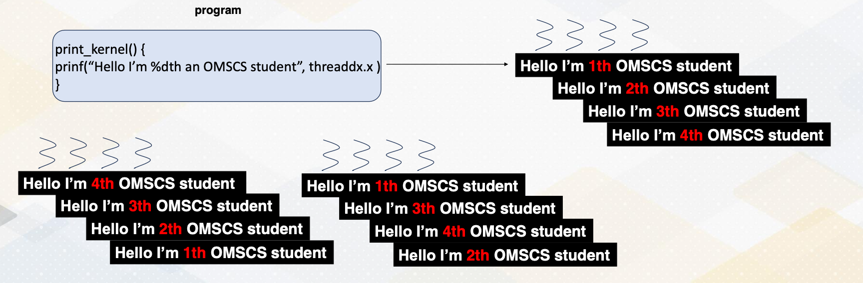
SPMD
Remember that GPUs execute code concurrently following single program multiple data SPMD paradigm.
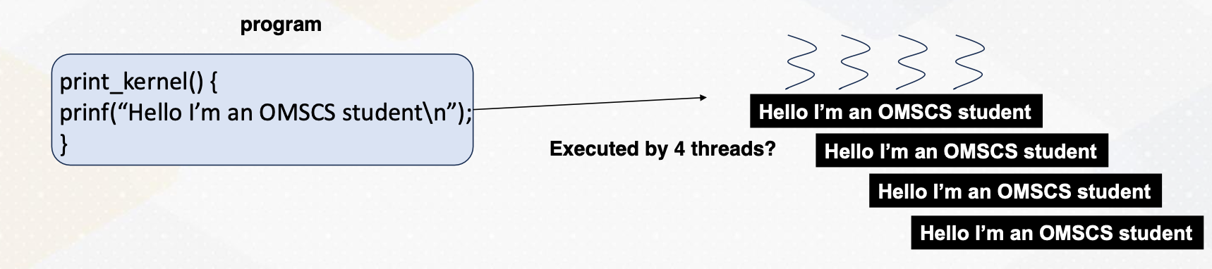
In this program, four threads were executed in parallel, each printing the message “hello, I’m an OMSCS student” without any specific ordering. However, we need to make each thread execute different data.
threadIdx.x
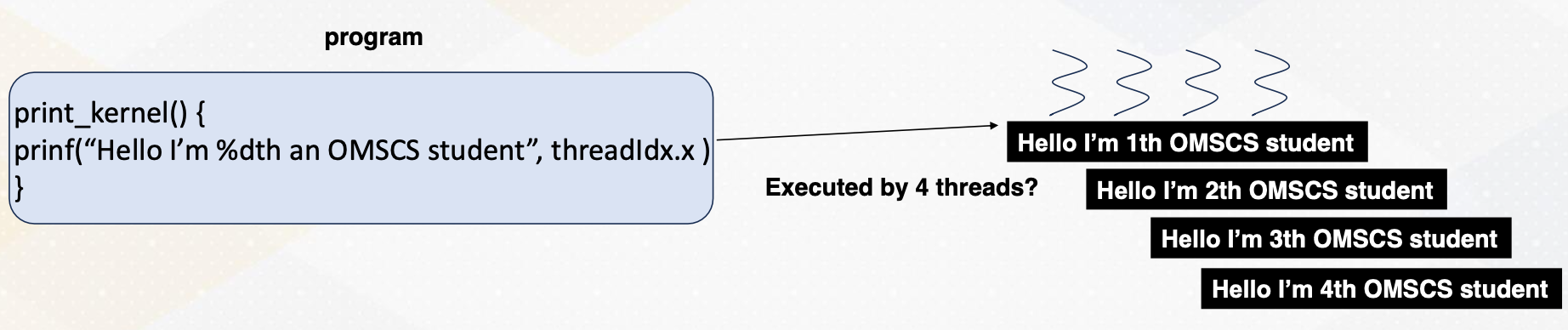
To offload different tasks per thread, we must assign unique identifiers to each thread. These identifiers are represented by built-in variables such as threadIdx.x, which represents the x-axis coordinate. This way each thread operates on different elements, enabling parallel processing even with a single program.
Vector Add with Thread Ids
1
2
3
4

vectorAdd (/* arguments should come here */) {
  int idx= threadIdx.x; //* simplified version */
  c[idx] = a[idx] + b[idx]
}
Now, returning to vector addition, we notice that it utilizes threadIdx.x. Each thread accesses a[idx] and b[idx] and idx is determined by thread ID. Therefore, this approach ensures that each thread operates on different element with the vector enhancing parallelism.
Execution Hierarchy
CUDA introduces complexity beyond the warps, a group of threads involving hierarchical execution.
Threads are grouped into blocks, and these blocks can be executed concurrently. This might be very confusing initially, since we already discussed that a group of threads are executed together as a warp. Warp is a micro architecture concept. In earlier CUDA programming, programmers do not have to know about the concept of warp because it was a pure hardware’s decision which we also call microarchitecture. Just note that in later CUDA, warp concept is also exposed to the programmer.
However, block is a critical component of CUDA,
- a group of threads form of block.
- Blocks and threads have different memory access scopes, which we will discuss shortly.
- CUDA block: a group of threads that are executed concurrently.
- Because of the different memory scope, data is divided among blocks.
- To make it simple, let’s assume that each block is executed on one streaming multiprocessor (SM).
- There is no guaranteed order of execution among CUDA blocks.
Example of Data indexing
-
threadIdx.x,threadIdx.y,threadIdx.z:threadindex -
blockIdx.x,blockIdx.y: block index
1
2
3
4

vectorAdd (/* arguments should come here */) {
  int idx= blockIdx.x * blockDim.x + threadIdx.x;
  c[idx] = a[idx] + b[idx]
}
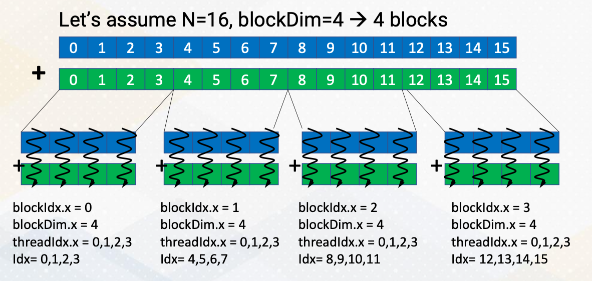
Let’s discuss an example where we divide 16 vector elements into four blocks. Each block contains four elements. ThreadId.x y z indicate thread index, similar to x, y, z coordinates. And blockId.x, y indicate block index, again similar to x and y coordinate. These indexes can be two dimensional or three dimensional and it can easily match with the physical size of images or 3D objects. To access all 16 elements, we combine block and thread IDs using block ID.x and threadId.x.
In this example, we divide 16 elements with four blocks. and each block has four threads. Each thread has unique ids, from 0 to 3 and each block has a unique id from 0 to 3 as well. Using the combination of these CUDA block ids and thread ids, we should be able to generate element index, idx. Idx equals blockId.x times blockDim.x plus threadId.x. This is a typical pattern of indexing elements using block idx and thread idx.
Shared memory
 The green dot represents on chip storage
Before we explore why this hierarchical execution is crucial, let’s discuss shared memory. Shared memory serves as a scratch pad memory managed by software. It is indicated as _shared_, it provides faster access compared to global memory which resides outside the chip. Shared memory is accessible only within a CUDA block. Here is an example of CUDA that shows shared memory.
1
2
3
4
5
6
7

// CUDA kernel to perform vector addition using shared memory
__global__ void vectorAdd(int* a, int* b, int* c) {
__shared__ int sharedMemory[N]; // Each thread loads an element from global memory into shared memory
Int idx = threadIdx.x;
sharedMemory[idx] = a[idx] + b[idx]; // Wait for all threads in the block to finish loading data into shared memory
__syncthreads(); // Perform the addition using data from shared memory c[idx] = sharedMemory[idx];
}
Execution Ordering: Threads
This slide also illustrates the threads are executed in any order. The print message can be 4, 3, 2, 1 or 1, 3, 4, 2, or 1, 2, 3, 4 threads.
Execution Ordering: Blocks
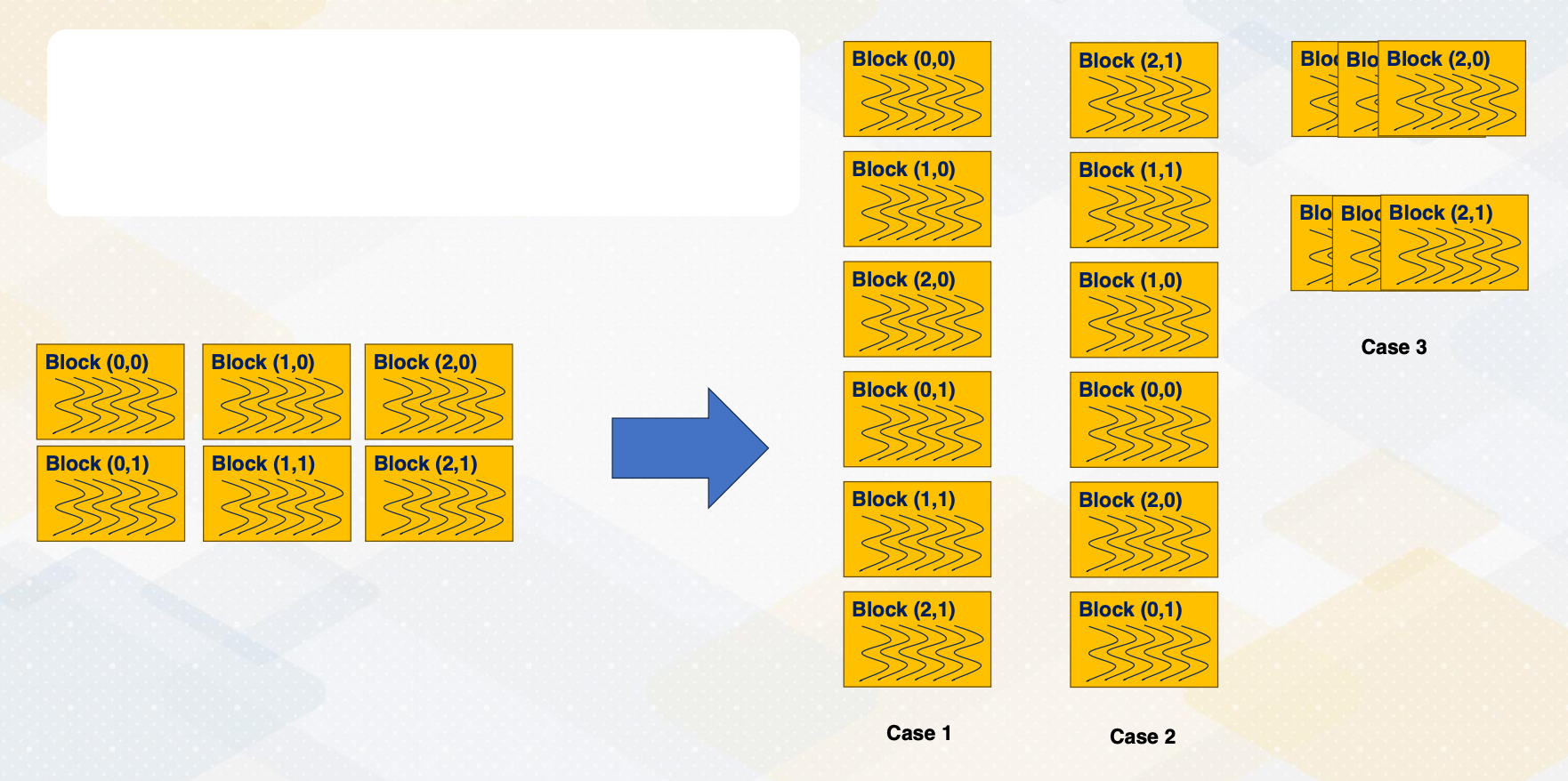
CUDA block execution also does not follow a specific order.
- Blocks can execute in any sequence, such as ascending order in case 1,
- descending order in case 2,
- and case 3, three blocks are executed together.
Thread Synchronizations
1
2
3
4
5

__global__ void Kernel(){
// work-1
__synchthreads(); // synchronization
// work-2
}
Since threads are executed in any order and can make progress with different speeds, to ensure synchronization among threads, we often use __sync_threads(), which synchronizes all threads until a specified point in the code. Interblock synchronization is achieved through different kernel launches.
Typical Usage with Thread Synchronizations
The typical computation pattern involves loading data into shared memory, performing computations, and storing results. So load from the global memory to the shared memory, compute with the data in the shared memory, and then store the results into the global memory back. This programming model is called BSP, Bulk Synchronous Parallel.
1
2
3
4
5
6
7

__global__ void Kernel(){
// Load to shared memory
__synchthreads(); // synchronization
// compute
__synchthreads(); // synchronization
// store
}
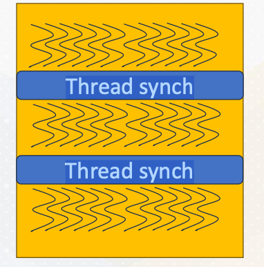
All threads work independently and then it meets at the thread synchronization point. This slide also shows these three step computation example and also illustrates threads and thread synchronization. Due to potential data dependencies and threads can be executed in any order, thread synchronization is vital.
Kernel Lanuch
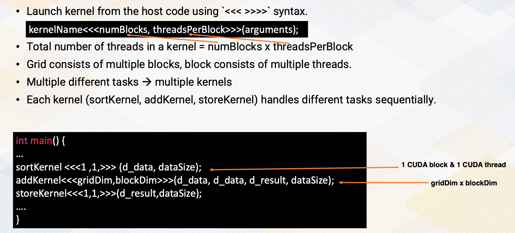
Now let’s discuss kernel launch again. Kernel launch is initiated from the host code with three angle brackets and specifies the number of blocks and threads per block. The total number of threads in the grid is the product of these two values. Grid consists of multiple blocks and block is consisted of multiple threads.
1
2
3
4
5
6
7

int main() {
...
sortKernel <<<1 ,1,>>> (d_data, dataSize); // 1 Cuda Block & 1 Cuda Thread
addKernel<<<gridDim,blockDim>>>(d_data, d_data, d_result, dataSize); // gridDim x blockDim
storeKernel<<<1,1,>>>(d_result,dataSize);
...
}
Here in this example, it shows three different kernels, sort, add, and store to handle three different tasks. One more thing to note is that sort is done using only one thread. And then the main add computation is done with gridDim times blockDim, number of threads, and then store is also done with only one thread. Here is an example to show that multiple kernels can be used for different tasks with its grid and block dimensions.
Memory Space and Block/Thread
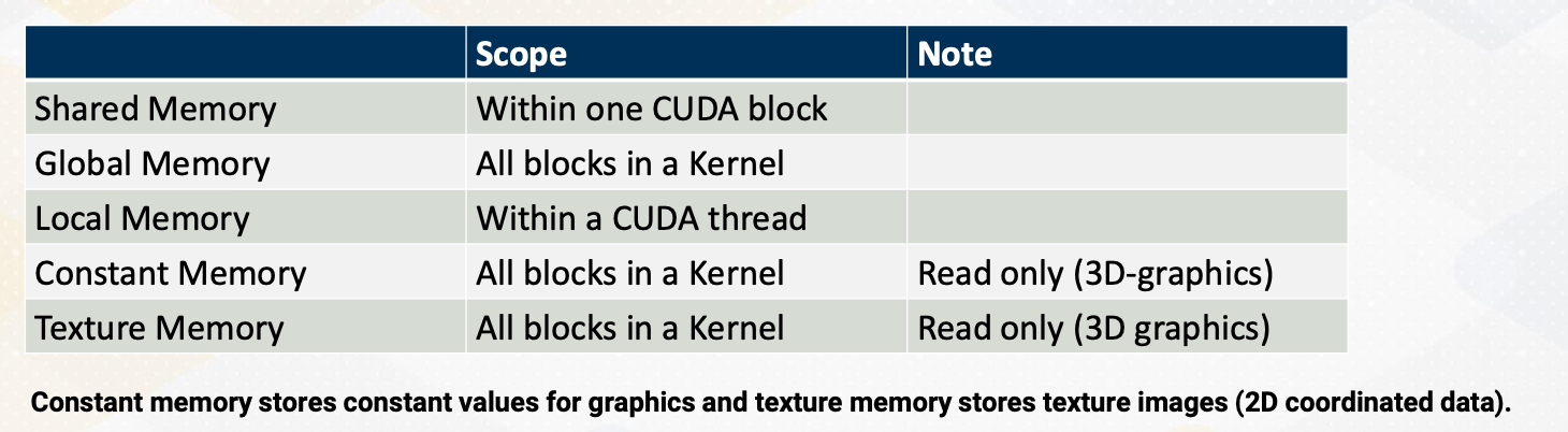
Here is a summary of memory space and block/thread. Shared memory is available only within one CUDA block, and global memory is accessible by all blocks in a kernel. Local memory is only within a CUDA thread. Constant and texture are from 3D graphics. And constant memory is very small and stores very small amount of read only data such as the value of fhi. Texture memory is also read only but it also stores texture values. So it’s structured for two dimensional accesses. For CUDA programmers, constant and texture memories are not widely used, so we will not discuss too much.
Information sharing is limited across CUDA execution hierarchy. This is probably the crucial reason to have different execution hierarchy. Data in the shared memory is visible only within one CUDA, which means the data in the shared memory can stay only in one SM (cpu core). Which also means that data in the shared memory of one CUDA block needs explicit communication. And later we will discuss that CUDA also support thread block cluster to allow data sharing in the shared memory.
Module 3 Lesson 2: Occupancy
Course Learning Objectives:
- Explain the concept of occupancy
- Determine how many CUDA blocks can run on one Streaming Multiprocessor
How Many CUDA Blocks on One Stream Multiprocessor?
So far, we have assumed that each SM handles a single CUDA block, but the reality is much more complex. Multiple blocks can coexist on a single SM, but how many? Two blocks per SM or three blocks per SM? What decides this choice?
Occupancy
How many CUDA blocks can be executed on one SM can be decided by the following factors.
- Number of registers,
- shared memory, and
- number of threads.
Exact hardware configurations are varied by GPU microarchitecture and different by each generation.
Let’s take a closer look at one example. We will explore the example with 256 threads and 64 kilobyte of register files and 32 kilobytes of shared memory.
- In the software side, each CUDA block has 32 threads and two kilobytes of shared memory, and each thread has 64 registers.
- If the occupancy is constrained by running number of threads, the total number of CUDA blocks per SM would be 256/32, which means eight CUDA blocks.
- If the occupancy is constrained by the registers, it will be 641,024/6432, which means 32 CUDA blocks.
- If the occupancy is constrained by the shared memory size, it will be 32 kilobyte divided by 2 kilobyte equals 16 CUDA blocks.
- So the final answer is the minimum of all constraints, so it will be 8 CUDA blocks per SM.
Number of Threads Per CUDA Block
- Host sets the number of threads per CUDA block, such as threadsPerBlock:
1

kernelName<<<numBlocks, threadsPerBlock>>>(arguments);
- Set up at the kernel launch time
- When it launches the kernel, the number of registers per CUDA block can be varied. Why?
- Because the compiler sets how many architecture registers are needed for each CUDA block. This will be also covered later part of this course.
- In case of CPU, the number of ISA decide the number of registers per thread such as 32. But in CUDA, this number varies.
- Shared memory size is also determined from the code.
- For example, the code says
__shared__ int sharedMemory[1000];. So in this case four byte times 1,000 equals 4,000 bytes. (Remember int is 4 bytes) So the occupancy is determined by these factors.
Why Do We Care about Occupancy?
Then why does the occupancy matter?
- This is because higher occupancy means more parallelism.
- Utilization - Utilizing more hardware resource generally leads to better performance.
- Exceptional cases will be studied in later lectures.
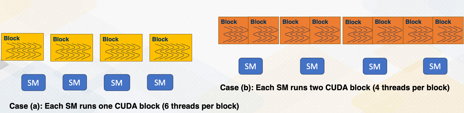
In case A, only one CUDA block runs on each SM, and each CUDA block has six threads. In case B, each SM can execute two blocks, but each block has only four thread. So total eight threads per block is running per each SM, which is actually more than case A.
- Case A - 4 * 1 * 6 = 24
- Case B - 4 * 2 * 4 = 32
Module 3 Lesson 3: Host Code
Course Learning Objectives:
- Write the host code for vector addition operation
- Explain the management of global memory
Managing Global Memory
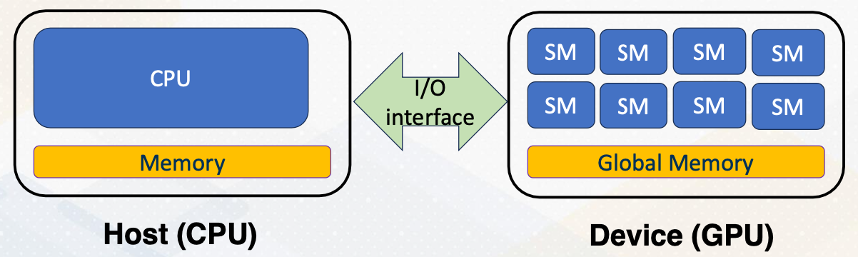
Recap, we have discussed that shared memory is visible within only CUDA block. And global memory is visible among all CUDA blocks. But this global memory is located at the device memory, which is not visible on CPU side because they are connected with I/O interface. Hence, there should be explicit APIs to manage device memory from the host side.
Managing Global Memory (cont’d)
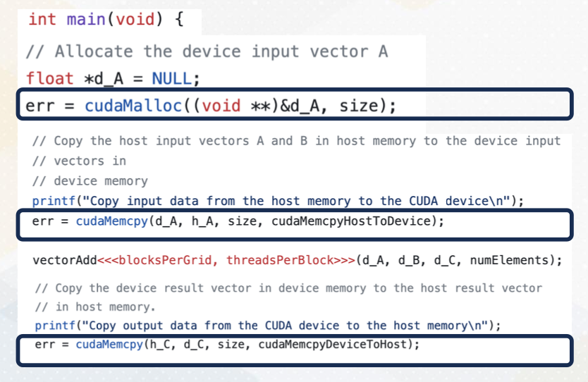
In this vector code example, we see two APIs that manage global memory. cudaMalloc and cudaMemcpy. cudaMalloc allocates memory in the GPU. In this example, cudaMalloc allocates d_A with the size. cudaMemcpy transfers data between CPU and GPU, either using cudaMemcpytoHostto Device or cudamemcpyDevicetoHost. Later lecture we will discuss using unified memory which eliminates the need for explicit data copies.
Review Vector Addition
Now this is a full vector addition code. In the left side we have a kernel code which is executed by individual threads on GPUs. And on the right side it shows a host code which is executed on CPUs.
Module 3 Lesson 4: Stencil Operation with CUDA
Course Learning Objectives:
- Be able to write a stencil code with CUDA shared memory and synchronization
Recap: Stencil Operations
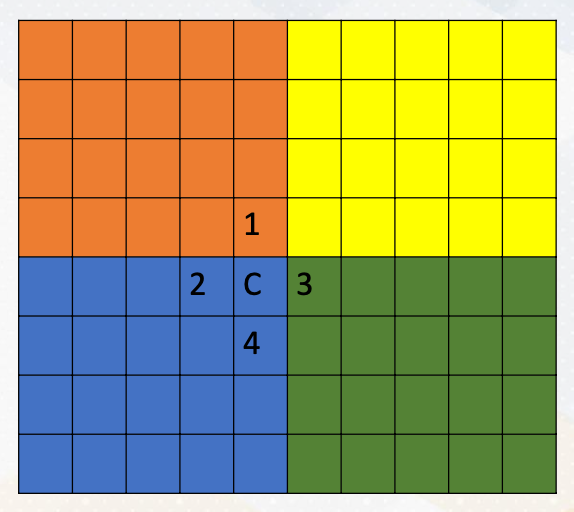
As we discussed in earlier videos, stencil operations are common operations in high performance computing. For example, here, C value is computed by simply averaging 4 neighborhood elements East, West, North, and South.
Each CUDA block performs different elements. Different color zones represent the area that is computed by each CUDA block. So this follows data decomposition programming pattern. Each thread handles one element of the stencil operation. And the operation will be fully parallel.
You also notice that one element will be used at least four times. So these are good candidates for caching, and since programmers know the exact pattern of reuse it is good to utilize the shared memory to store in an on-chip storage.
Stencil Operations: Operations Per Thread
Let’s use the shared memory for stencil operation. As we discussed, typical way of using shared memory is three stages.
- In the first stage, the processor loads data from global memory to the shared memory, on-chip storage.
- In the second stage, the processor actually performs stencil operation.
- In the third stage, the processor writes the result back eventually to the global memory.
- Typically thread synchronizations are between Stage 1 and Stage 2 to make sure the computation is performed after all the shared memory is loaded from the global memory.
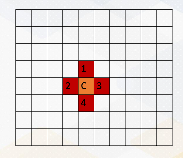
How about Boundaries?
Using shared memory exposes another problem. If you remember shared memory is only accessible within one CUDA block. If we divide the memory area by colors, each CUDA block can access its own color zone. However, to compute the value in C location, we need the element in Location 1 in red area, 3 in green area.
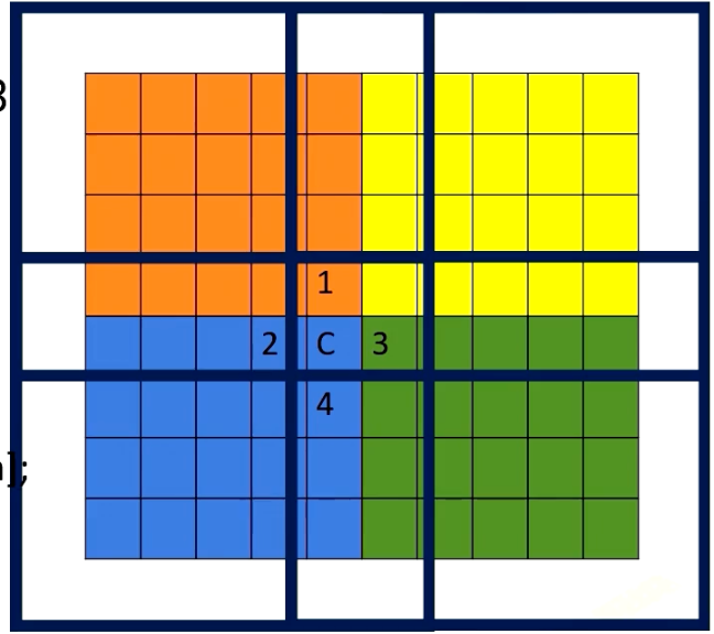
Hence, the way it works is each shared memory brings boundary elements as well, such as the following. This is a somewhat similar to MPI programming where explicit communications are needed for boundaries. Here in CUDA, we just simply bring boundary data to the shared memory. We can do that because we make sure those data is only read only data. Here we show an example of using shared memory for stencil operation. Please note that to make the example more simpler, we use a filter to compute stencil operation, which is similar programming style with convolutional operations.
1
2
3
4

// Load data into shared memory
__shared__ float sharedInput[sharedDim][sharedDim];
int sharedX = threadIdx.x + filterSize / 2;
int sharedY = threadIdx.y + filterSize / 2;
Use if-else to Check Boundary or Not
Maybe it looks obvious, but it was not clearly mentioned earlier. Is that if-else statement can be also used in the CUDA programming. Depending on the position of x, y values, the program can also decide whether it brings the data from the global memory or it fills with zero. This is implemented with if-else statement to check whether thread ID is belonged to a certain range.
The program has to create more number of threads than actual color zone and threads only within the inner element. The original color zone area performs computation. In other words, more threads are created to bring the data from the global memory to the shared memory. The bottom code example shows the actual computation snippet again, This code uses convolutional operation style to make the example have less if-else statements.
- Load different values on boundaries
1
2
3
4
5

if (x >= 0 && x < width && y >= 0 && y < height) {
sharedInput[sharedY][sharedX] = input[y * width + x];
} else {
sharedInput[sharedY][sharedX] = 0.0f; // Handle boundary conditions
}
- Perform computations only on inner elements
1
2
3
4
5
6

// Apply the filter to the pixel and its neighbors using shared memory
for (int i = 0; i < filterSize; i++) {
for (int j = 0; j < filterSize; j++) {
  result += sharedInput[threadIdx.y + i][threadIdx.x + j] * filter[i][j];
}
}
Module 4: GPU Architecture
Objectives
- Describe GPU microarchitecture
- Be able to explain the basic GPU architecture terminologies
Readings
Module 4 Lesson 1: Multi-threaded Architecture
Course Learning Objectives:
- Explain the difference between multithreading and context switch
- Describe resource requirements for GPU multithreading
In this module, we’ll dive deeper into GPU architecture. Throughout this video, we’ll explore the distinctions between multithreading and context switching in GPUs. We’ll also discuss resource requirements for GPU multithreading.
Recap: GPU
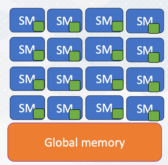
Let’s first recap the fundamentals of GPU architecture.
- GPUs are equipped with numerous cores.
- Each core features multithreading,
- which facilitates the execution of warp or wave front within the core.
- Each core also has shared memory and hardware caches.
Multithreading
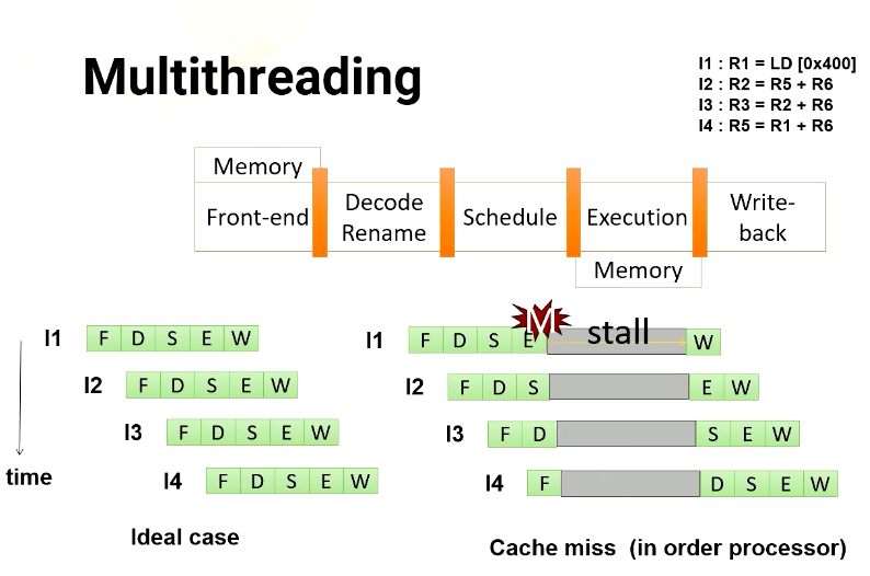
Let’s dive into multithreading. Imagine a GPU with a five stage pipeline and four instructions. In an ideal scenario, each instruction would proceed through the pipeline one stage at a time. However, in an in order processor, if an instruction has a cache miss, the following instructions have to wait until the first instruction completes. If you look carefully, the instruction 2 is not actually dependent on instruction 1. Hence, in an out of order processor, instruction 2 doesn’t have to wait.
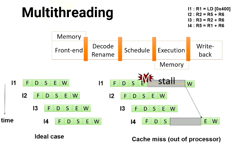
So in an out of order processor, it starts to execute instruction 2 and 3 before instruction 1 completes. Once instruction 1 receives the memory request, instruction 4 can be executed.
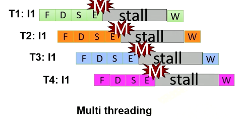
In multithreading, the processor just simply switches to another thread regardless of whether a previous instruction generates cache misses or not. Since they are from different threads, they’re all independent. In this example, the processor executes four instructions from four different threads. Furthermore, the processor also generate four memory requests concurrently.
Benefits of multithreading
To get the benefit of generating multiple memory requests, GPU utilize multithreading. Instead of waiting for stalled instructions, GPU start to execute instructions from another thread, allowing for parallel execution as well as more memory requests.
- Multithreading’s advantage is its ability to hide processor stall time, which is often contributed by
- cache misses,
- branch instructions or
- long latency instructions such as ALU instructions.
- GPUs leverage multithreading to mitigate such long latency issues.
- While CPUs employ out of order execution, cache systems, and instruction level parallelism (ILP) to tackle latency.
- Longer memory latency requires a greater number of threads to hide latency
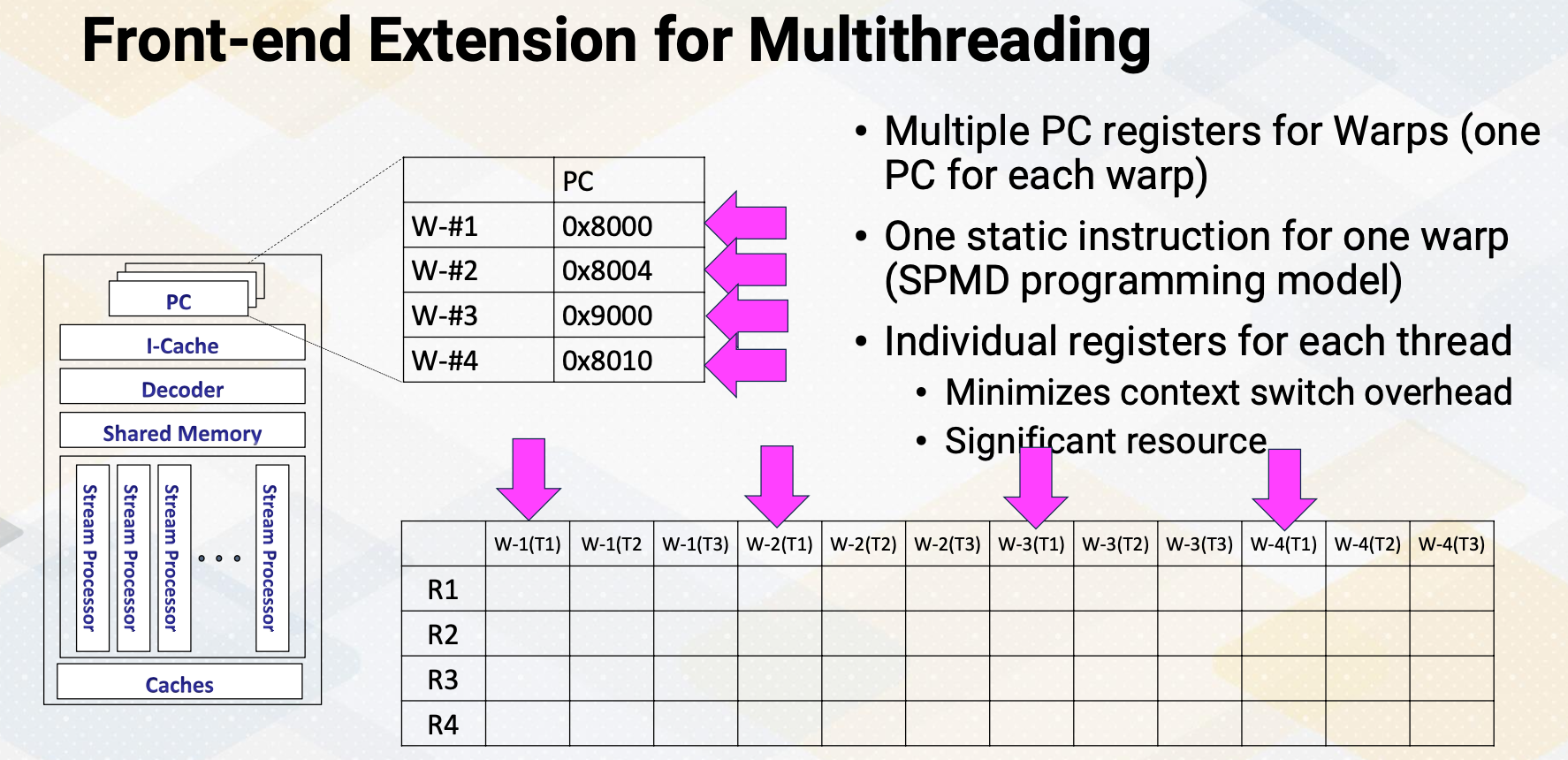
Front-end Extension for Multithreading
The front end features multiple program counter (PC) values, each warp needs one PC register so supporting four warps requires four registers. It also has four sets of registers. So context switching in GPUs, means simply switching the pointer among multiple PC registers and register files.
CPU Context Switching
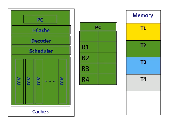
In contrast, CPUs implement context switches in a different way. When executing a thread, the instruction pipeline, PCs, and registers are dedicated to the specific thread.
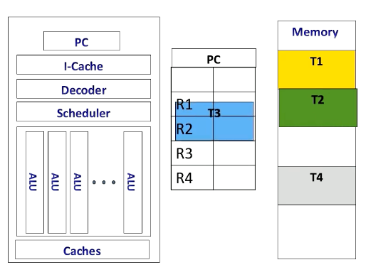
If the CPU switches to another thread, for example, from T2 to T3, it stores T2’s contents in memory and loads T3 content from the memory.
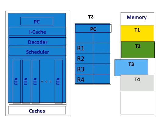
Once it’s done, it executes the original thread context. Context switches in CPUs incur substantial performance overhead due to the need to store and retrieve register contents from the memory.
Hardware Support for Multithreading
Now let’s discuss the resourc e requirement for multithreading in more detail.
- Front-end needs to have multiple PCs
- One PC for each warp since all threads in a warp share the same PC
- Later GPUs have other advanced features, we’ll keep it simple and assume one PC per warp.
- Additionally, a large register file is needed.
- Each thread needs “K” number of architecture registers
- total register file size requirement = K times $\times$ number of threads
- “K” varies by applications
- Remember occupancy calculation?
- Each SM (shared memory) can execute Y number of threads, Z number of registers, etc.
- Here, Y is related to the number of PC registers. So if the hardware has five PC registers, it can support up to 5 times 32, which is 160 threads.
- Z is related to K
Revisit Previous Occupancy Calculation Example
Let’s revisit a previous example to calculate occupancy. If we can execute 256 threads, have 64 times 1024 registers and 32 kilobytes of shared memory, here 32 threads per warp is assumed. And then the question is how many PCs are needed?
- The answer is 256 divided by 32, which is eight PCs.
If a program has 10 instructions, how many times does one SM need to fetch an instruction?
- The answer is simply put, 10 multiplied by 8 which is 80.
Module 4 Lesson 2: Bank Conflicts
Course Learning Objectives:
- Explain SIMT behavior of register file accesses and shared memory accesses
- Describe techniques to enhance bandwidth in register and shared memory accesses
CUDA Block/Threads/Warps
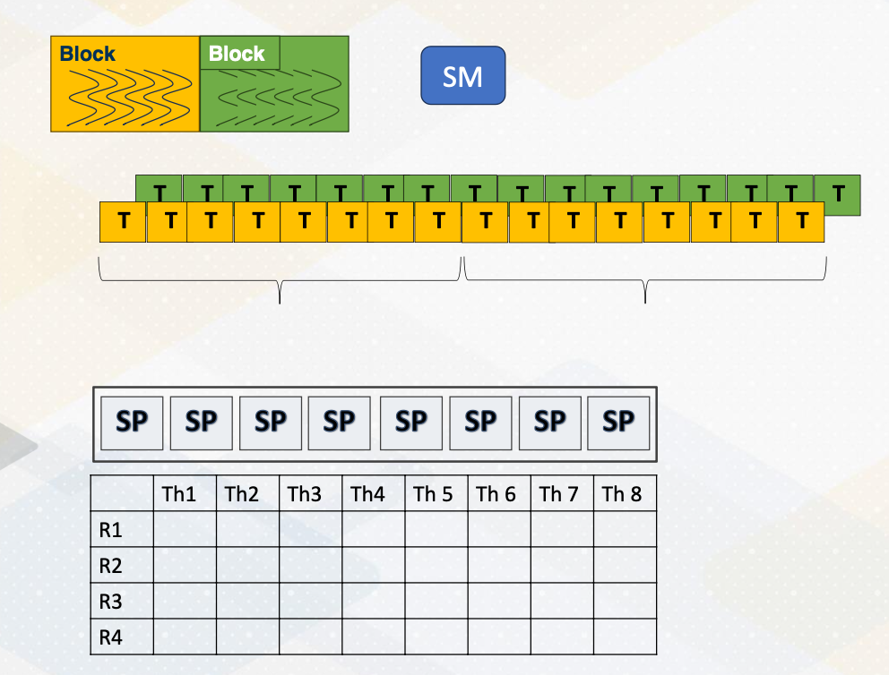
Let’s revisit GPU architecture basics. In a GPU, multiple CUDA blocks run on one multiprocessor and each block has multiple threads. And a group of threads are executed as a warp. As shown in this animation, one warp will be executed and then the other warp will be executed. Each thread in a warp needs to access the registers because the registers are per thread. Assume that each instruction needs to read two source operands and write one operand and the execution width is eight. In that case, we need to supply eight times three, two read and one write which is 24 values at one time.
Port vs Bank
Let’s provide some backgrounds about ports and bank. Port is a hardware interface for data access. For example, each thread requires two read and one write ports. And if an execution width is a four, then there is a total of eight read ports and four write ports.
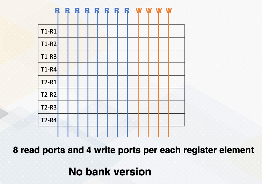
This figure illustrates eight read ports and four write ports per each register element. Read and write ports literally require wires to be connected. So it actually uses up quite a bit of space.
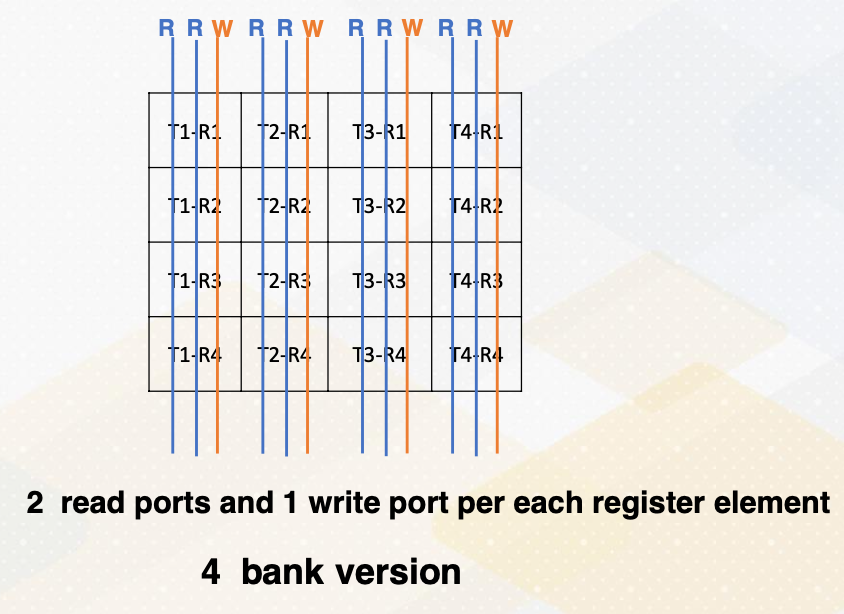
On the other hand, we can place register files differently and put only two read ports and one write port for each register element. This is called a four bank version which requires a much smaller number of ports.
What is a bank? Bank is a partition or a group of the register file. The benefit of bank is that multiple banks can be accessed simultaneously which means we do not need to have all read and write ports. We can simply have multiple banks with fewer read and write ports as shown in these diagrams. This is important because more ports means more hardware wiring, and more resource usage.
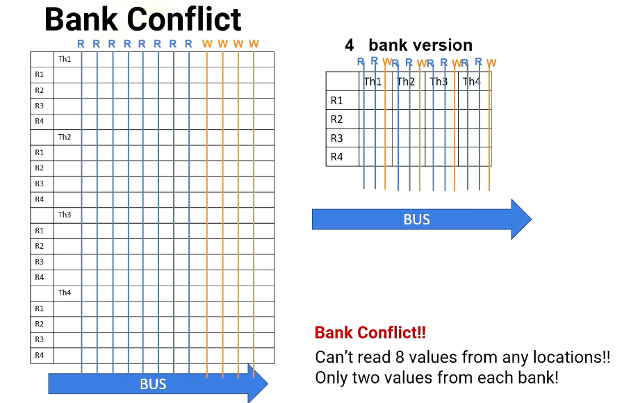
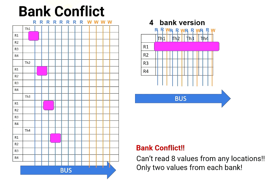
Bank conflict
 Scenario #1: read R1 from T1,T2,T3,T4 (each thread on different banks)
However, a challenge arises when multiple threads in a warp requires simultaneous access to the same bank, which causes bank conflict. For example, in Scenario 1, the processor needs to read R1 from thread 1, 2, 3, 4. And each thread register file is on different bank.
 Scenario #1: read R1 from T1,T2,T3,T4 (each thread on different banks)
In no bank version it has eight read ports. So it can easily provide four read values, as does the four bank version, since all register file accesses are in different banks.
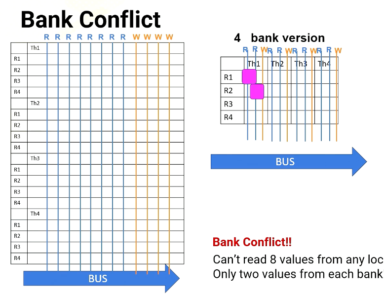 Scenario #2: read R1, R2, R3, R4 from T1
However, in Scenario 2, the processor has to read from R1, R2, R3, and R4. All are in the same thread or in the same bank. For 8 port version, no problem. It can read all four values simultaneously, but in the four bank version it can read only two values at a time. So it takes multiple cycles.
Variable Number of Registers per Thread
- Will Register File Have Bank Conflicts?
- Why do we worry about bank conflicts for registers? Don’t we always need to access two registers from different threads anyway?
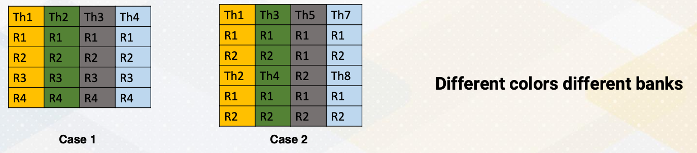
The challenge arise because CUDA programming will get benefits from different register counts per thread. Let’s say that we want to operate instruction R3 = R1+R2. Here are two cases.
- In the first case, four registers per one thread.
- In the second case, two registers per one thread. And different colors means different banks.
- In Case 1, reading registers would not cause a bank conflict because each thr ead register file is located in a different bank.
- However, in Case 2, read R1, R2 from multiple threads would cause a bank conflict because thread 1 and thread 2 are in the same bank. Same for Thread 3 and Thread 4.
- Remember, GPU executes a group of threads (warp), so multiple threads are reading the same registers. Then how to overcome this problem? The first solution is using a compile time optimization.
Solutions to Overcome Register Bank Conflict
Then how to overcome this problem? The first solution is using a compile time optimization. The compiler can optimize code layout because register ID is known as static time.
Side Bar: Static vs. Dynamic
Let me just provide a little bit of background of static versus dynamic. In this course static often means before running code. The property is not dependent on input of the program. Dynamic means that the property is dependent on input of the program.
Here is an example. There is a code ADD and BREQ.
1
2

LOOP: ADD R1 R1 #1
    BREQ R1, 10, LOOP
Here is an example. There is a code ADD and BREQ. Let’s say that this loop iterates 10 times. What would be static and dynamic number of instructions? Static number of instruction is 2, since this is what we see in the code, and dynamic number of instruction is 2 times 10 becomes 20. Also note that static time analysis means compile time analysis.
Solutions to Overcome Register Bank Conflict (Cont)
Going back to the solution to overcome register bank conflict, we try to use compile time analysis to change the instruction order or to remove bank conflict. But not all bank conflicts can be avoided.
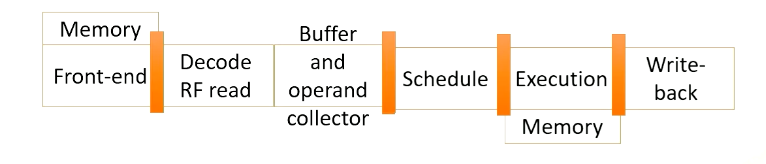
So in a real GPU, GPU pipeline is more complex (beyond a 5-stage pipeline). First, register file access might take more than one cycle, maybe there is a bank conflict, or maybe because the register file might have only one read port, so the pipeline is actually expanded.
After value is read, the values are stored in a buffer. After that, scoreboard is used to select instructions.
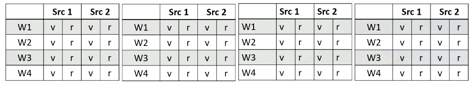
Scoreboarding
Scoreboard is widely used in CPUs to enable out of order execution. It is used for dynamic instruction scheduling.
However, in GPUs, it is used to check whether all source operands within a warp are ready and then it chooses which one to send to the execution unit among multiple warps. Possible policies is oldest first, and there could be many other policies to select warps.
Reading Register Values
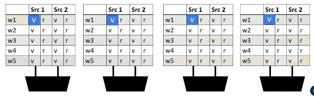
Here is an example. Reading register files might take a few cycles. Ready register values are stored at a buffer. And this diagram shows the buffer and scoreboard.
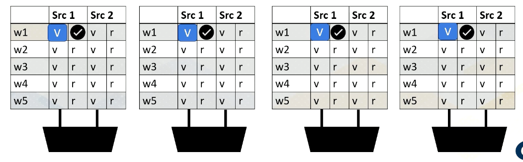
Whenever a value is stored, it sets the ready bit. Here, Warp 1, src 1 is ready.
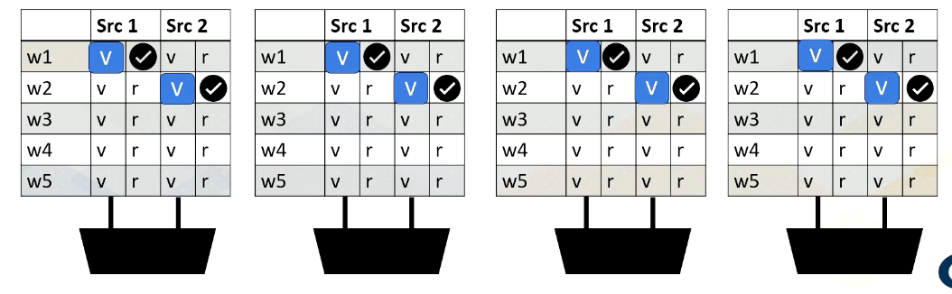
then Warp 2, src 2 is ready,
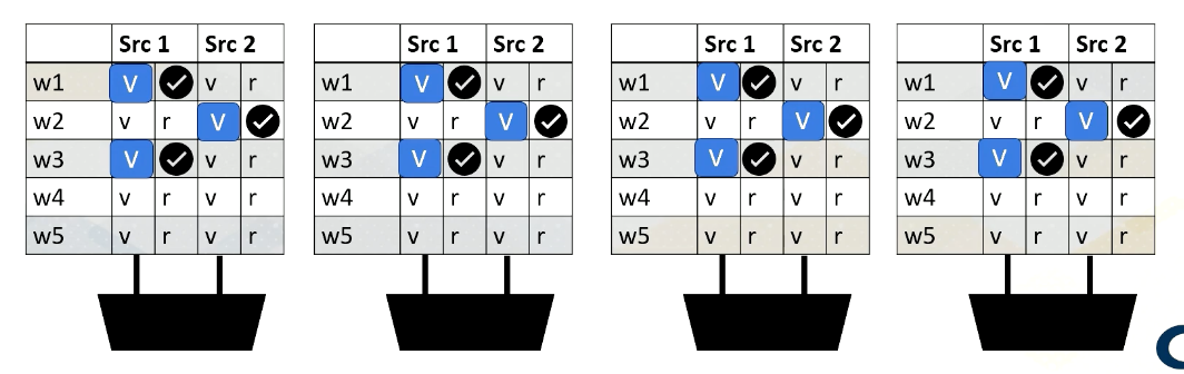
then Warp 3, src 1,
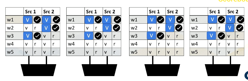
and then finally Warp 1, src 2 are ready.
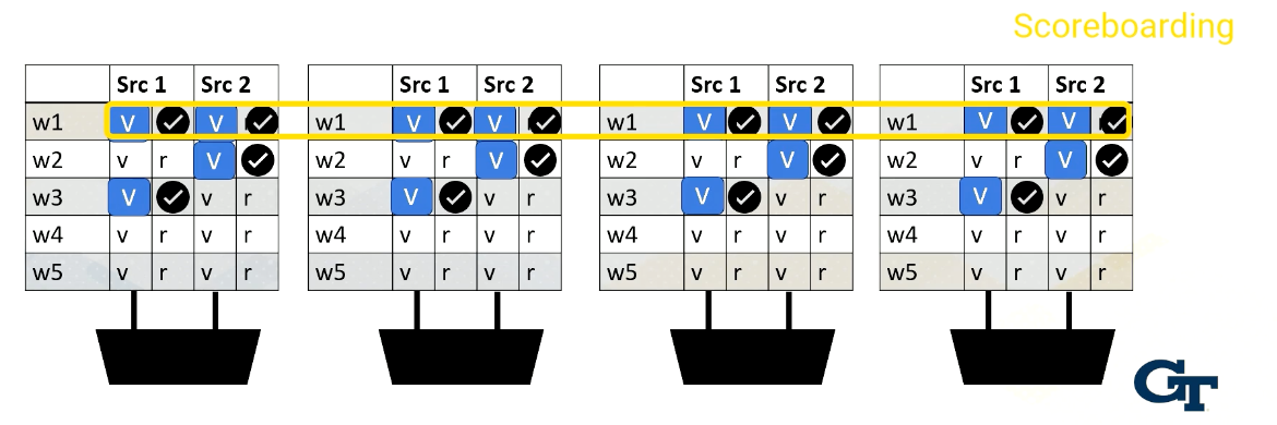
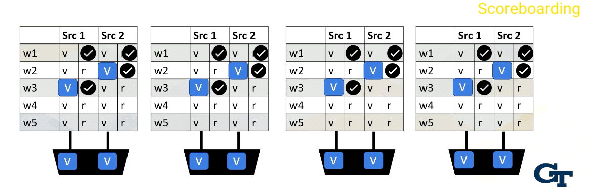
When all values are ready, the scoreboard selects the warp, then the values are sent to the execution unit.
Shared Memory Bank Conflicts
Bank conflict can also happen in the shared memory on GPUs. Shared memory is on-chip storage and also scratch pad memory. Shared memory is also composed with banks to provide high memory bandwidth. Let’s assume the following shared memory.
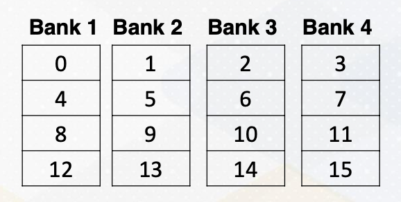
There are four banks and the number in a box represent memory addresses.
Here is a code which shows shared memory, shared input.
1
2

__shared__ float sharedInput[index1];
Index1= threadIdX.x *4
And the index to the shared memory is computed by simply multiplying threadIdX.x and 4. Which means that thread 1 needs to access memory address 4, and thread 2needs to access memory address 8, and thread 3 needs to access memory address 12, and so on. Unfortunately, all these addresses are all mapped to the same bank, so all threads will generate bank conflicts. The solution is changing the software structure, which we will cover more in later lectures.
In summary, in this video, we have learned the benefits of banks in register and shared memory. We have also studied the reasons of bank conflicts in register files and shared memory.
Module 4 Lesson 3: GPU Architecture Pipeline
Course Learning Objectives:
- Describe GPU pipeline behavior ith multithreading and register file access
- Explain how mask bits are used.
GPU Pipeline (1)
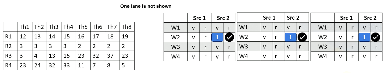
Here is a GPU pipeline.
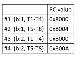
Here it shows PC values for each warp. In this example, there are four warps, and the first warp should fetch from PC value 0x8000 and the first warp is from Block 1 and threads 1-4. The second warp is from Block 1 as well and threads 5-8. The third warp is from Block 2 and threads 1-4, and fourth warp is Block 2 threads 5-8.
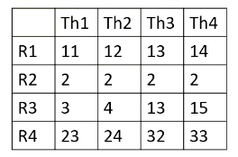
Here it shows register values for Block 1.
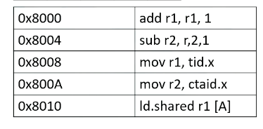
Here it shows an I-cache memory address and the instructions. You see tid.x at 8008. Tid.x is a special register to store thread ID within a block. And an instruction at 8000A has a ctaid, which is another special register to store block ID within a grid.
And here is a scoreboard. Okay, the front end fetches an instruction from 8000. Only one instruction is fetched for entire warp. Add r1, r1, 1.
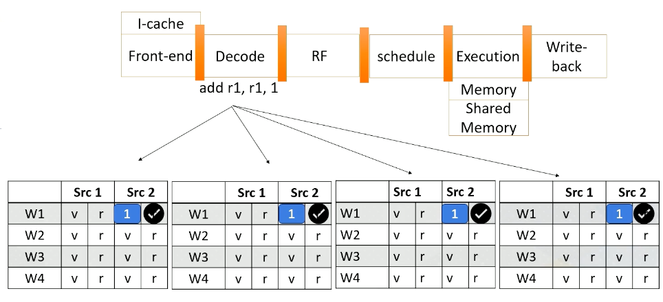
This instruction is brought to the front end, and then it is sent to the decode stage, and it will be decoded. Since the instruction itself has a constant value or immediate value 1, the value 1 will be broadcasted to the scoreboard.
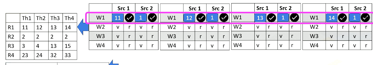
So all source 2 operands are ready for the warp 1. And in the register file access stage, we access the source register 1, which is r1 for thread 1, 2, 3, 4. And values are read and sent to the scoreboard. So now, the processor checks the instruction and sees that all the source operands are ready, so this warp is selected.
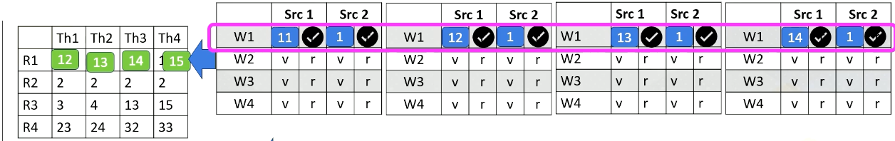
The warp is sent to the execution stage and it performs the additions, and the final result will be written back to the register file at the right back stage.
GPU Pipeline (2)
Now let’s look at the second warp. It fetches an instruction from warp 2 which is Block 1 and thread 5-8. Again, the instruction is decoded, the constant value 1 is broadcasted to all source operand buffers. Here we omit the values for one execution unit due to the space limitation.
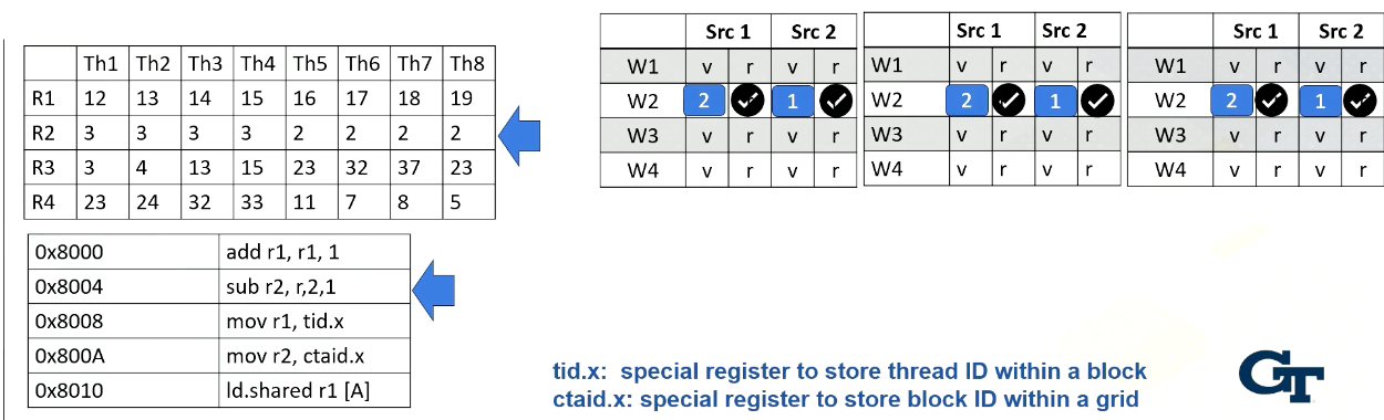
In the next stage, the processor accesses the register file and reads value r2 from thread 5-8. In this example, all source values are all two. Now all source operands are ready, so the scheduler select Warp 2 and they will be executed even though they are all operating in the same values.
The hardware performs the same work for all thread in a warp, in the subtractions and perform 2 minus 1. And then the result will be written back at the write back stage just like the previous example. They will update the register values for thread 5-8.
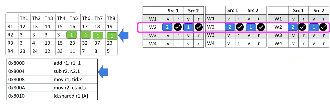
GPU Pipeline (3)
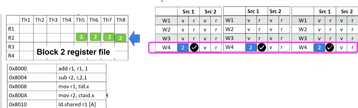
Now let’s assume the processor fetches from warp 4. The PC address is 8000A, which moves ctid.x to r2, The warp 4’s block ID is 2, so ctid.x value is also 2. Ctaid.x value is read and stored inside the scoreboard. These values will be stored to r2 at the write back stage as shown in this animation.
GPU Pipeline (4)

Now, let’s assume that instead of 8000A, the processor fetches from 8008 for warp 4. The instruction has tid.x. Since this is for threads 5-8, tid.x values will be 5, 6, 7, and 8. The tid.x values will be read and stored in the scoreboard, and in the write back stage, all these values will be written back to r1 as shown in this animation.
Mask bits
What if we do not need to execute r4 threads? GPU stores information, tells which thread or lane is active. One ALU execution path is called lane.
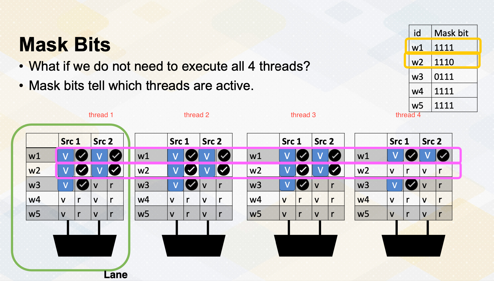
Active thread performs actual computation and inactive thread will not do any work. Mask bits tell which threads are active or not. Here scoreboard shows register values and ready bits. Warp 1 has 1111 in the mask bit, which means all threads in the warp 1 will actually perform the work. Warp 1 is selected and is executed. In the warp 2 case, the mask bit is 1110, so only the first three lanes or first three threads will do the work.
In summary, in this video we have reviewed the GPU pipeline’s instruction flow. We also studied the use of special registers for thread ID and block ID. The concept of active mask for identifying active SIMT lanes is also introduced in this video.
Module 4 Lesson 4: Global Memory Coalescing
Course Learning Objectives:
- Explore global memory accesses
- Explain Memory address coalescing
- Describe how one warp can generate multiple memory requests
Let’s look at more on global memory coalescing. In this video, we’ll explore global memory accesses. You should be able to explain memory address coalescing and you should be able to describe how one warp can generate multiple memory requests.
Global Memory accesses
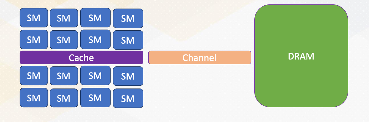
Here the slide illustrates GPU and DRAM. In GPU architecture, one memory instruction could generate many memory requests to DRAM because one warp can generate up to 32 memory requests if we assume warp size is 32. So the total number of memory requests can easily be a larger number. For example, if we have 32 SMs and each SM has one warp to be executed, 32 times 32 In other words, 1024 requests can be generated in one cycle. Each memory request is 64 byte, so 64 kilobyte per cycle, and if we assume one GHz GPU, 64 terabyte per second memory bandwidth is needed.
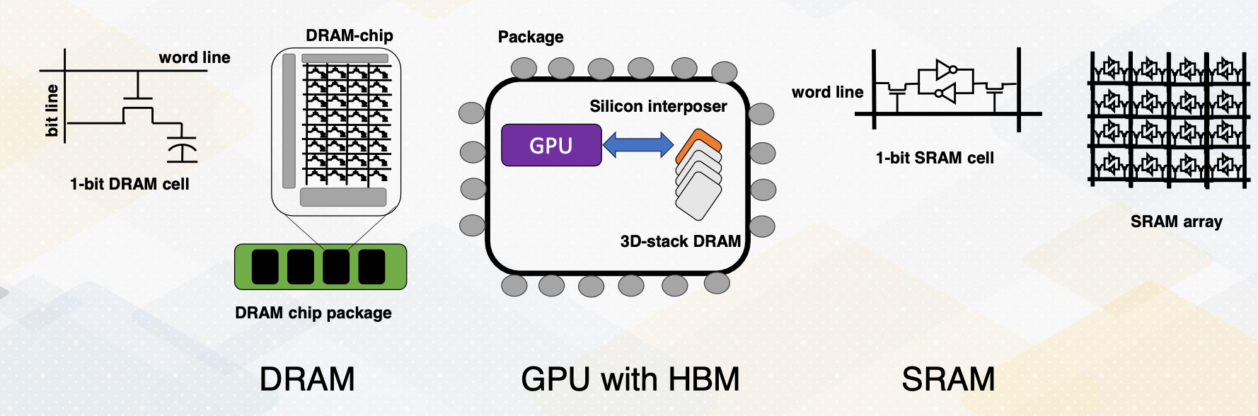
Side Bar: DRAM vs. SRAM
Let me briefly provide a background on DRAM and SRAM. SRAM is composed of six transistors and combining multiple one bit SRAM cell makes SRAM, and SRAM is commonly used in caches. On the other hand, DRAM is composed of one bit transistor and DRAM chip has many one bit DRAM cells. Since each bit requires only one bit DRAM, DRAM can provide a large capacity but all communication in the DRAM chip require pins to communicate which can be a limiting factor.
HBM overcomes this problem. First, by stacking DRAM, it provides much higher density of DRAM. Then, by connecting memory with GPUs using silicon interposer, it avoids off chip communication. So all communications between GPU and DRAM are all inside the same package. Hence, HBM provides a significant amount of memory bandwidth.
Memory Coalescing
Even if the memory can provide high memory bandwidth, reducing memory request is still critical to performance. Because GPU cache is very small. It’s very easy to saturate memory bandwidth. Here is an example of two global memory accesses.
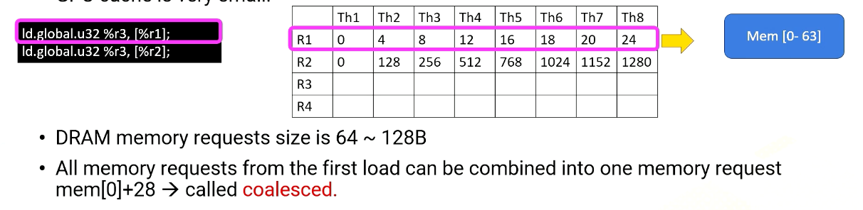
The first instruction, Ld.global, it uses register value R1 to generate memory addresses. R1’s content within a warp is all sequential so the memory addresses are all sequential too. Therefore, all memory requests from the first load can be combined into one memory request, memory 0-28 or 0-63. And this is called coalesced.
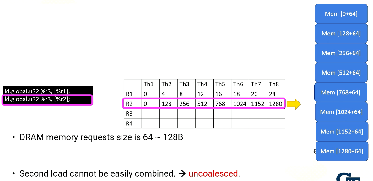
On the other hand, the second load which looks the same as the first instruction, but the content of R2 is quite different, the R2 values are all stride apart by 128. So each memory request needs to be sent separately. Second load cannot be easily combined, which is called uncoalesced.
Coalesced Memory
Coalesced memory combines multiple memory requests into a single or more efficient memory request. Consecutive memory requests can be coalesced. Coalesced memory reduces the total number of memory request. This is one of the key software optimization techniques.
In summary, uncoalesced global memory requires significant amount of performance, so they can degrade the performance significantly. GPUs have the potential to saturate memory bandwidth because of a large number of concurrently running threads. Coalescing memory requests is crucial for efficient memory accesses and better GPU performance. <!– <iframe class=”embed-video” loading=”lazy” src=”https://www.youtube.com/embed/10oQMHadGos” title=”YouTube video player” frameborder=”0” allow=”accelerometer; autoplay; clipboard-write; encrypted-media; gyroscope; picture-in-picture” allowfullscreen
</iframe> –>
Module 5: Advanced GPU Programming
Objectives
- Describe GPU microarchitecture
- Be able to explain the basic GPU architecture terminologies
Readings
Required readings
- General-Purpose Graphics Processor Architectures ( Synthesis Lectures on Computer Architecture), Chapter 3 site.
- CUDA best practices (sections 9, 10, 11)
- Shared memory
- For Project #2 preparation
Optional Suggested Readings:
- Nvisight
- NSight doc
- NVIDIA presentation
- CUDA stream
- Data transfer
- NSight Compute Video Series
- NSight Blog
Module 5 Lesson 1: Advanced GPU Programming
Course Learning Objectives:
- Describe GPU optimization techniques
- Prepare for advanced technique materials
This video will provide an overview of various techniques to optimize the performance of GPUs so that you will be ready to read more advanced techniques in the reading list. This techniques will help you to optimize your GPU programming project.
Applications Suitable for GPUs
GPUs are good for tasks:
- Involving massive parallel data to take advantage of massive number of threads.
- Applications that have low dominance in host device communication costs are good for running on GPUs.
- Furthermore, applications that have coalesced data accesses in the global memory accesses are good for running on GPUs.
Profiling
- enables us to identify performance bottlenecks by identifying hotspots in our applications.
- It provides key performance metrics such as
- reported throughput,
- the number of divergent branches,
- the number of divergent memory, both coalesced and uncoalesced,
- occupancy,
- and memory bandwidth utilization.
To achieve this, please use profilers provided by GPU vendors to analyze and optimize our kernel functions. Profiling is also useful before you convert your applications for GPUs to identify the key hotspots in CPUs.
Optimization Techniques
- GPU execution time can be broken into data transfer time, memory access time, and compute time.
- Hence, we have to look at all three aspects to optimize applications.
- Reducing data transfer time,
- optimizing memory access patterns,
- and reducing computation overhead.
- Finally, if possible, please use provided libraries.
Data Transfer Optimizations
First, optimizing data transfer overhead between host and device is critical. Data transfer overhead occurs of using host and device memory connection fabric and it had, typically, a high overhead such as PCI-E. Since such overhead can be very harmful, faster communication is still actively developed.
The figure in this slide illustrates the timeline for data copy and kernel execution.
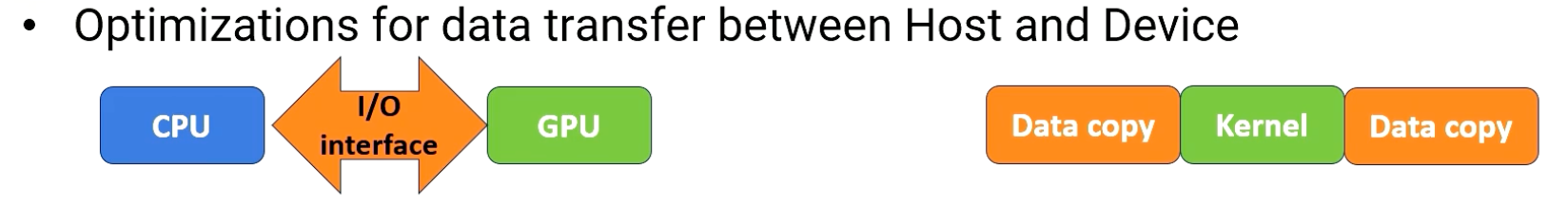
There are several methods to optimize.
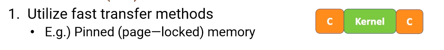
First, if possible, use the fast transfer methods such as pinned memory. With pinned memory, it reduces the data copy time by reducing the overhead from the CPU side. Now, the data copy time box gets smaller.
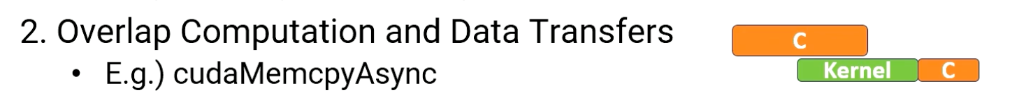
Second, overlap computation and data transfer. cudaMemcpyAsync API can be used for this purpose. The diagram shows that data copy and kernel compute time is overlapped.
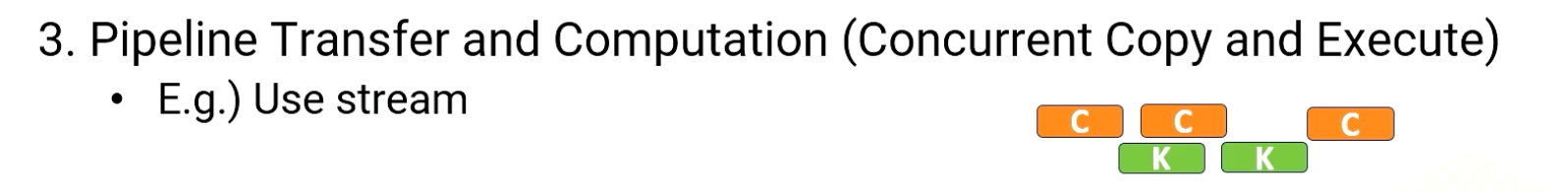
Third, pipeline the data transfer and computations or it is also referred as concurrent copy and execute. This can be achieved by using stream feature in CUDA. This often requires breaking kernel and copy into multiple sessions.
Fourth, use direct host memory access if possible.
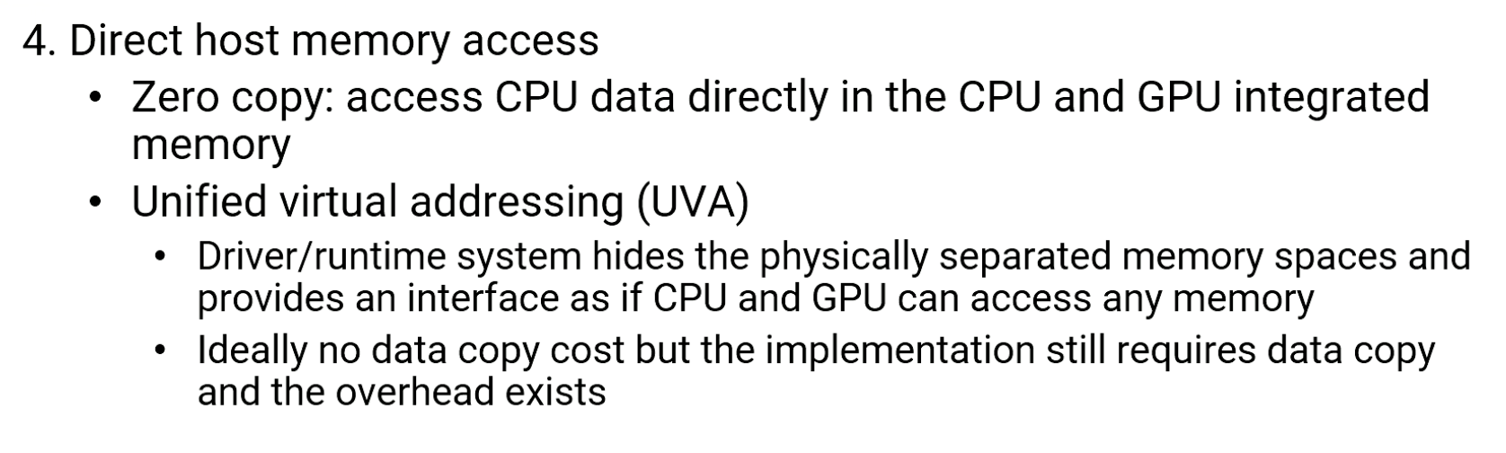
- Zero copy allows access CPU data directly in the CPU and GPU integrated memory.
- Next, use unified virtual addressing, UVA. We’ll discuss UVA again later.
- Briefly, in the UVA, driver and runtime system hide the physically separated memory spaces and provide an interface as if CPU and GPU can access any memory as if they are sharing the same memory space.
- Ideally, there should be no data copy cost, but the implementation still requires data copy, so the overhead exists.
Not all these methods are applicable for all applications. Programmers need to try out different methods based on their systems and their target applications.
Memory Access Pattern Optimizations
One of the most important optimization opportunities is reducing the global memory access overhead.
- First, if possible, utilize cache as much as possible.
- Second, make sure all global memory accesses can be coalesced and also aligned.
- Reducing the number of data memory transactions is the key of optimizing for the performance.
- Also check the average memory bandwidth consumption to see whether an application is fully taking advantage of memory’s peak bandwidth.
- Lastly, reduce shared memory bank conflict.
Reduce Computation Overhead
- Reducing the competition overhead is also very important.
- You can use instruction level optimization, such as replacing the high cost instructions with the low cost instructions.
- As an example, use shift operations instead of multiplications or divisions.
- Second, use low precisions when possible, or use fewer number of bits, such as single precision or 16 bits, or even using 8 bits, if that’s allowable.
- Next, use hardware built in special functions that are provided by the hardware such as rsqrtf() function.
- Utilizing math libraries often provide these opportunities automatically
- Reduce the branch statement
- use predicated execution if possible
- Avoid atomic operations if possible.
- The overhead of atomic operation has been reduced significantly, but still it is better to avoid.
- Use tensor operations and utilize the tensor cores.
- Again, if we are using libraries, it will typically use tensor cores whenever they are possible.
Newer CUDA Features
Let me also introduce a couple of newer CUDA features. Several warp level operations exist, such as warp shuffle, vote, ballot, etc. Modern GPUs have been adding new warp-level operations.
- This is because communication between threads is very expensive.
- Since register files are unique to the thread, there is no easy way of accessing other threads’ register contents without using shared memory.
- That requires movement between register to shared memory and then back to register files which might also cause shared memory bank conflict.
- Hence, new hardware features are provided to allow data movement within a warp.
The figure illustrates the register values are swapped between threads. There are also other features, like cooperative groups, to utilize different formation of warps.
Also, newer GPUs provide smaller warp-level operations instead of fixed warp sizes.
- For example, independent thread scheduling was introduced in Volta architecture.
These new features are making:
- GPUs be apart from SIMT execution. It even allows each thread could have different pieces and different thread group execution.
- In this course, we assumed shared memory is only accessible by only one CUDA block, but in newer GPU, this is no longer true.
- It can specify that shared memory can be shared by multiple CUDA blocks. This makes more sense if those CUDA blocks are all scheduled to the same hardware SM.
- As a newer feature, unified memory for shared memory, L1 data cache, and texture memory are also introduced.
- And hardware acceleration for split arrive/wait barriers are also introduced since synchronization is quite expensive in many cases.
Cuda libraries
We also highlight continuously developing CUDA libraries including:
- cuBLAS for linear algebra,
- cuSPARSE for sparse matrices,
- cuTENSOR for tensor based linear algebra.
- Thrust for parallel algorithms and communication libraries like NCCL and NVSHMEM for multi GPU setups.
- Deep learning programs will benefit from libraries like a cuDNN.
Please refer to latest library documentation to see more details.
Other GPU Programming Platforms
Although this course focuses on using CUDA, there are many other programming languages and platforms libraries such as OpenCL, OneAPI/SysCL, OpenACC, HIP, Kokkos, and even popular languages like Python and Julia. These libraries open up programming GPU other than using CUDA.
In summary, GPU programming optimization require reducing the amount of computation, reducing data transfer overhead between the host and device, and ensuring efficient memory access patterns in both global and shared memory. These techniques are essential for achieving the full potential of GPU performance.
Module 6: GPU Architecture Optimizations - I
Objectives
- Describe the performance issues related to divergent branches and the basic mechanisms for handling them.
- Describe the opportunities for GPU register optimization.
- Explain the differences between shared memory and register files.
- Develop the ability to read GPU architecture papers
Readings
Required Readings:
- General-Purpose Graphics Processor Architectures ( Synthesis Lectures on Computer Architecture), Chaper 3 Georgia Tech Library access
- Wilson W. L. Fung, Ivan Sham, George Yuan, and Tor M. Aamodt. Dynamic warp formation and scheduling for efficient GPU control flow. In Proc. of the ACM/IEEE International Symposium on Microarchitecture (MICRO), pages 407–420, 2007.
- Hyeran Jeon, Gokul Subramanian Ravi, Nam Sung Kim, and Murali Annavaram. GPU register file virtualization. In Proc. of the ACM/IEEE International Symposium on Microarchitecture (MICRO), pages 420–432, 2015. DOI: 10.1145/2830772.2830784. 64.
- Mark Gebhart, Stephen W. Keckler, Brucek Khailany, Ronny Krashinsky, William J. Dally: Unifying Primary Cache, Scratch, and Register File Memories in a Throughput Processor. MICRO 2012: 96-106
Optional Readings:
- V. Narasiman, M. Shebanow, C. J. Lee, R. Miftakhutdinov, O. Mutlu and Y. N. Patt, “Improving GPU performance via large warps and two-level warp scheduling,” 2011 44th Annual IEEE/ACM International Symposium on Microarchitecture (MICRO), Porto Alegre, Brazil, 2011, pp. 308-317.
- Mark Gebhart, Daniel R. Johnson, David Tarjan, Stephen W. Keckler, William J. Dally, Erik Lindholm, and Kevin Skadron. 2011. Energy-efficient mechanisms for managing thread context in throughput processors. In Proceedings of the 38th annual international symposium on Computer architecture (ISCA ‘11). Association for Computing Machinery, New York, NY, USA, 235–246.
- M. Gebhart, S. W. Keckler, and W. J. Dally, “A Compile-Time Managed Multi-Level Register File Hierarchy,” in International Symposium on Microarchitecture, December 2011, pp. 465–476.
Module 6 Lesson 1: Handling Divergent Branch
Course Learning Objectives:
- Explain the definition of divergent warps
- Apply hardware techniques to handle divergent warps
In this video, let’s discuss divergent warps and how hardware handles divergent warps.
Divergent branches
As you all know by now, warp is a group of threads that are executed together. So far, we have assumed that all threads in a warp would execute the same program following SPMD, single program multiple data programming model. However, it is also possible that threads might execute different parts of the program.
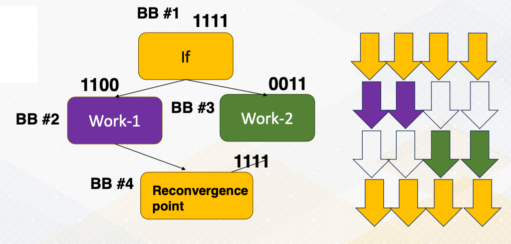
Example can be found from if-else st atement. There is an if-else statement and it checks whether thread ID is less than two or not in this slide example. This means that the thread ID less than two will execute one path, and the last will execute different path. Within a warp when not all threads need to fetch different parts of the program, it is called a divergent branch, and then the warp that executes divergent branch is called divergent warp.
In the divergent warps, we need to use active mask to indicate which threads are active or not. In the slide it shows that 1, 1, 1, 1 or 1, 1, 0, and these are indicating active mask bits, and which are next to the BB1 or two, and BB stands for basic block. The path is split after Basic Block 1, then it meets again at Basic Block 4. At the moment, all threads will be executed together again. And this point is called reconvergence point, and in the compiler’s term, it is called immediate post dominator.
If-else Conversion: Predicated Execution
If-else conversion or predicate execution. Divergent branches can be eliminated with if-else conversion or predicated execution. In predicated execution, instructions are predicated, and whether an instruction is executed or not is dependent on the predicate value.
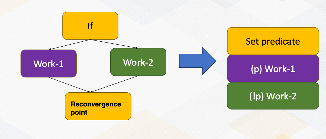
The diagram shows that if-else statements are converted as a predicate execution. Work 1 and Work 2 are predicated with an opposite of predicate value. This change is called if-else conversion, and this is commonly used in vector processors. A branch that has a small amount of work, In other words, Work 1 and Work 2 are small. Then if-else conversion is often used even in modern CPUs. The biggest downside of predicated execution is that the work that won’t be executed still needs to be fetched. So this if-else conversion needs to be used carefully if the amount of work such as Work 1 and Work P are really big.
GPU Execution Flow
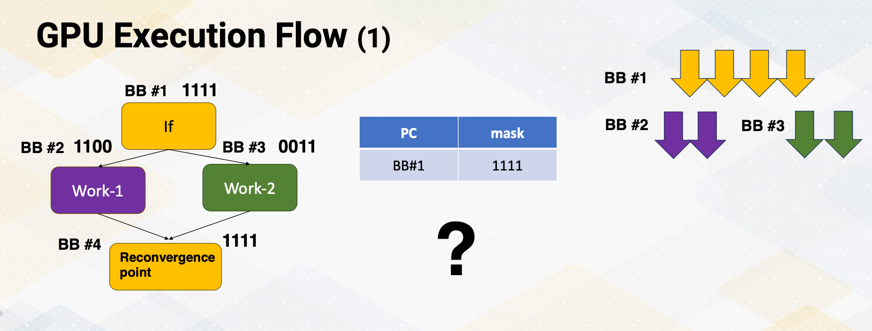
Hence, most sub branches still remain as a branch instruction, and they can be divergent. When a processor fetches an instruction, it computes the next instruction address. First, it can detect whether a branch is divergent or not based on whether all PC values within a warp are the same or not. When PC values are different, it becomes a divergent branch and it needs to be handled differently.
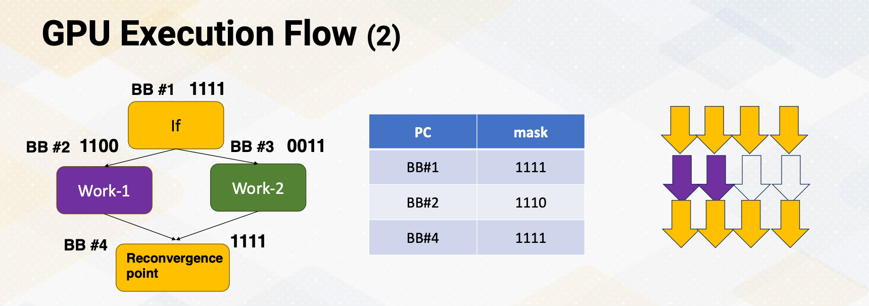
Let’s you assume that the processor fetches one path, in this case Basic Block 2 first. Once it executes Basic Block 2, then it will fetch execute Basic Block 4. In this scenario we are completely missing Basic Block 3. Now how should we know when to fetch Basic Block 3, and how to even know the address of Basic Block 3?
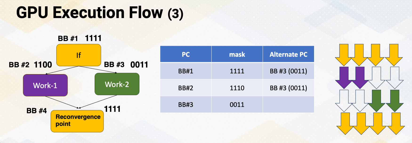
So to overcome this problem, when a processor fetches and it detects a divergent branch, it needs to store the other PC address. So basic block stores the alternative PC value which is Basic Block 3 in the same place.
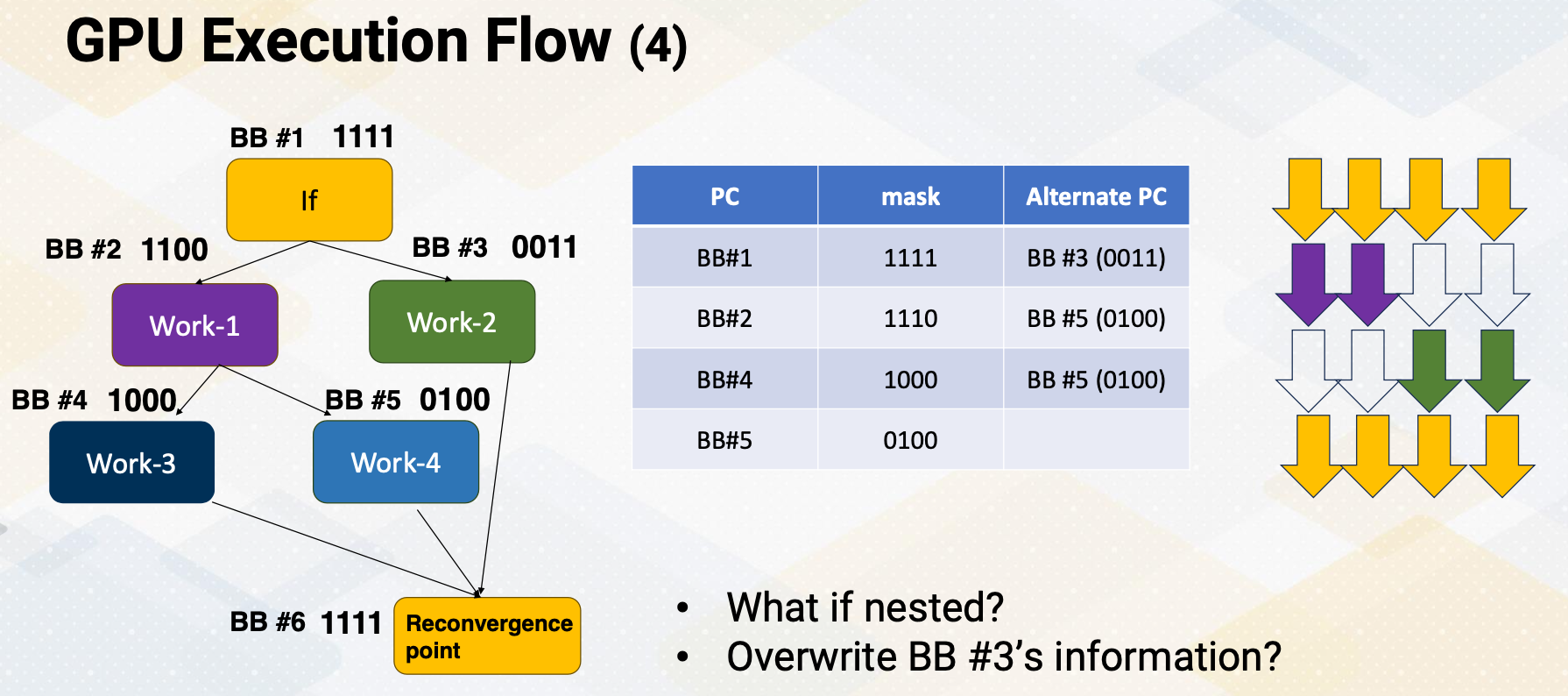
However, this problem gets even more complicated if control flow get complex. What if a Basic Block 2 also has a branch instruction? It is called the nested branch. If we only have one place to store alternative PC value, then the alternative PC value will be overwritten as a Basic Block 5. In that case, it will lose information of Basic Block 3. So how can you overcome this problem? You might think about handling nested function calls. Yes, this is very similar to do that.
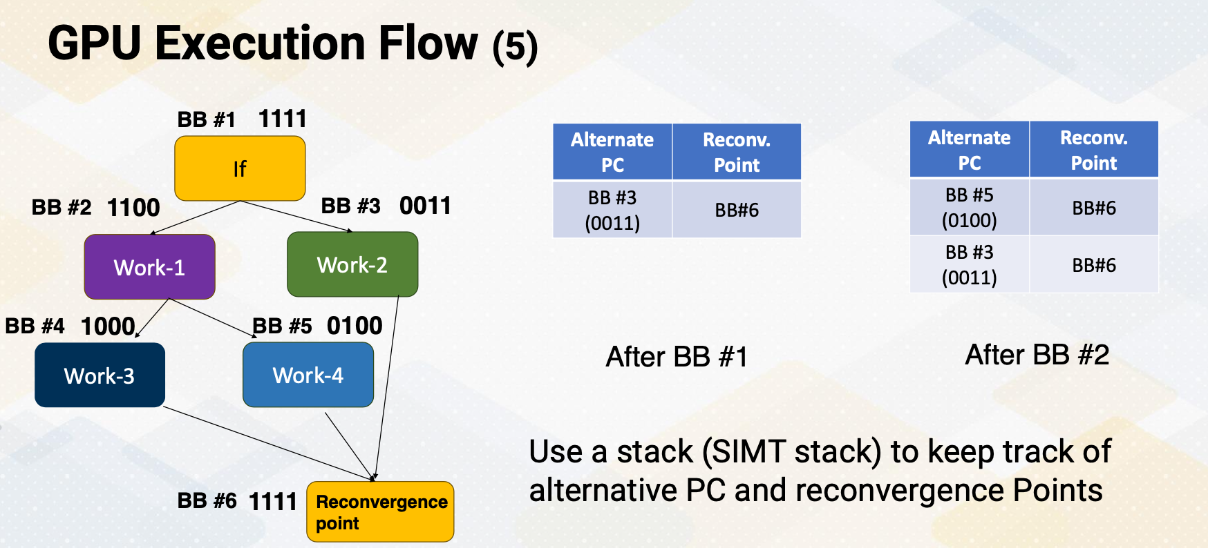
We can use stacks, and stacks are good operations to handle this kind of behavior. We put a stack to keep track of alternative PC values. After the Basic Block 1, the processor puts alternative PC value and also reconvergence point in a stack. When it fetches another divergent branch, it pushes a new alternative PC value and reconvergence point in a Stack 2, and it continues to fetch and execute. This stack is called the SIMT stack, because it is very critical to support SIMT, single instruction multiple thread. We need this kind of stack.
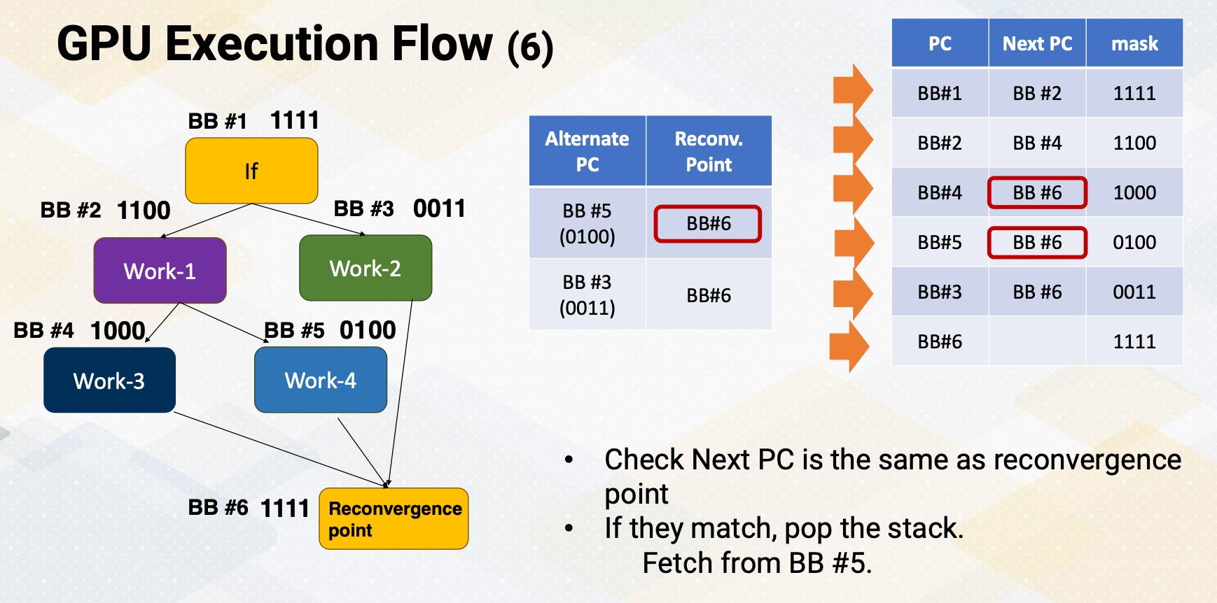
Once the processor knows that the next PC address is the same as the reconvergence point in a stack, it pops alternative PC values from a stack and it starts fetching from this alternative PC. Here, this slide animates the instruction fetch process. This shows the stream of instructions. First, the processor fetches Basic Block 1, and it detects that it is a divergent branch. So it stores alternative PC value and reconvergence points in the SIMT stack. The next PC is BB2. It fetches the next PC BB2, and then it detects that this is another divergent branch. So the divergent branch information is stored in a stack, and then it goes to next PC which is Basic Block 4. At the moment, if it compute next PC value and realize that next PC value is the same as the reconvergence point on the top of the stack. When the next PC value matches the top of the stack of reconvergence point, instead of fetching from next PC, it fetches from the alternative PC value. It pops Stack 2. So if fetches Basic Block 6, and then compute the next PC value. The next PC value of basic block is six, which is the same as reconvergence point of the top of the step. So in that case, again, it pops a stack and fetches from alternative PC value, which is Basic Block 3, and then it continues to follow the next PC values.
How to Know the Reconvergence Point?
Another question is how to identify this is reconvergence point, which is very critical to support the SIMT and divergent branches.
- It is typically done at compile time and static time, using control flow graph analysis. Compiler can insert a marker to indicate reconvergence point or compiler inserts special instruction to indicate that.
Typically hardware prefers to have a hardware stack to handle reconvergence point, it detects divergence and also stores reconvergence point purely based on hardware information.
- However, some cases compiler could insert explicit stack operation to specify when to push and pop this reconvergence point.
Downside of this compiler approach is, divergent branch information needs to be detected at compilation time, which is very hard. So they can overclaim more branches as divergent branches. So hardware prefer these one time operations.
Large Warps
- One thing to note that the width of warp is a micro architecture feature.
- The benefits of larger warps are
- one instruction’s fetch and execution can generate many number of execution instructions such as 32, 64, 120 etc.
- So larger width means it’s wide execution machines and wide vector processors.
- The downside is the chance of divergence is very high.
- A warp can be often easily be divergent, and when it’s divergent it needs to go through these complex SIMT fetch operations.
- And this is very specific to applications. Some application has more uniform execution width and path, and some application might have very frequent divergent branches. So we have to decide based on applications.
Dynamic Warp Formation
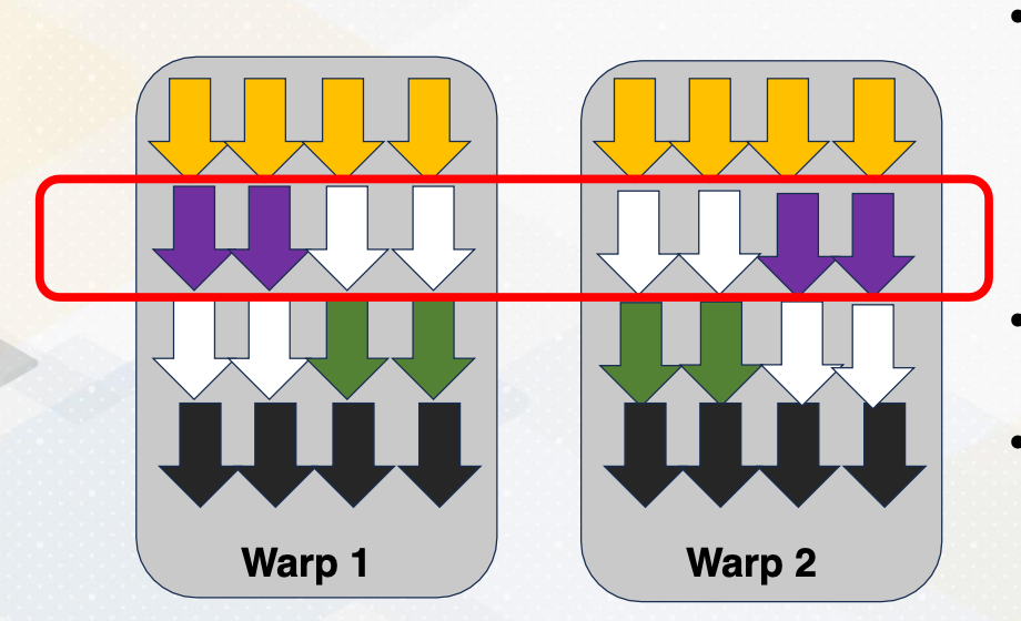
You might also notice that once a divergent warp exist, the execution utilization becomes very low. In this example, only half of the execution units are utilized. To overcome this problem, some hardware optimizations are proposed to regroup different threads from different warps. Because the threads excute the same PC, we can easily group them as the same warp, then we can execute them with very high execution width utilizations. This decision needs to be done by hardware and it is often called dynamic warp formation because we’re forming the warp at one time. There have been many optimizations that were proposed to increase the efficiency of this warp execution. And one of the critical challenges is how to avoid the register file conflict, because threads location within the warp often optimize to reduce register file read and write per conflict. When you regrouping this thread with the new warp, we have to preserve this conflict otherwise we might end up generating lots of register file conflicts.
In this lecture, we reviewed the concept of divergent branches. And we studied how GPU fetches divergent branches using SIMT stack. And we also studied the benefit of having large warps, and also we briefly studied the concept of dynamic warp formation, which are commonly used to optimize the hardware optimization performance.
Module 6 Lesson 2: Register Optimizations
Course Learning Objectives:
- Explain the challenges of register file sizes and opportunities
- Discuss various optimization techniques aimed at increasing the size of register files effectively
In this video, let’s discuss divergent warps and how hardware handles divergent warps.
In this video, we’ll continue learning GPU architecture optimization techniques focusing on register file optimizations. The learning objective of this video is to explain the challenges of register file sizes and opportunities and to discuss various optimization techniques aimed at increasing the size of register file efficiency.
Register File Challenges
- As you recall, each SM has a large number of threads and that number of threads also has many registers. The hardware has to keep track of the number of threads times the number of registers, which it can be 64 kilobyte, 128 kilobyte, or even 256 kilobyte.
- Large register size means it can be easily slow, and providing high bandwidth and fast latency is a very challenge.
- In the GPUs world, the register file read bandwidth should be equal to the execution bandwidth.
- We can utilize other computer architecture optimization techniques for the GPU register files.
- We could reduce the access latency by utilizing hierarchical approach to provide different access latency.
- We could also reduce the size by utilizing resource sharing.
Observation 1: Not All Threads are Active
First, let’s look at some GPU specific register file usage characteristics. GPUs have many thread, but not all threads are active. GPUs use SPMD programming model and all threads have the same register file usage from the program’s viewpoint. However, GPU execution is very asynchronous, so thread completion time varies a lot. Some threads might be finishing early, but some threads finish very late.
An interesting part is that the register files in the finished threads are no longer needed. Furthermore, as we studied in the previous video lecture, divergent branches execute different path of program which might result in different register file usages. So register file usage pattern can be varied at runtime.
Observation 2: Not All Registers are Live
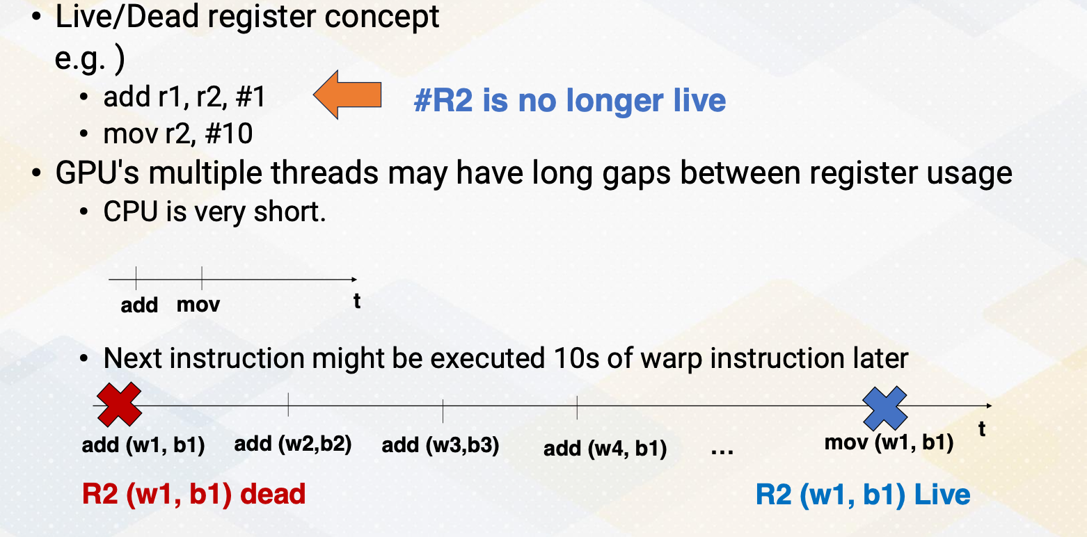
Another observation is that not all register are live. Live register means that the value in the register file will be used and dead register means that the value is no longer needed. For example, add r1, r2, 1 and move instruction r2, 10. R2 value in the add instruction is no longer live because r2 value will be overwritten in the move instruction. So r2 register is dead after add instruction.
You might think that this is not a big problem because in the CPU’s world, add instruction and move instructions are typically executed back to back, just like in this illustration. However, in the GPU’s case, the next instruction might be executed 10s of warp instruction later. Here is an animation. First, we execute add instruction from warp 1 and CUDA block 1. And then another add instruction from warp 2 and block 2. Another add instruction, warp 3 from block 3 and so on. We continue for a while until we execute add instruction on warp and block 1 again. So r2 in warp 1, block 1 is dead right after this first add instruction from the warp 1 and b1. And then, the move instruction is executed a long time later from the same thread, warp 1, block 1 and r2 becomes live at the moment. So this period between r2 is dead and live can be very long depending on the schedule’s execution pattern.
Observation 3: Short Distance between Instructions
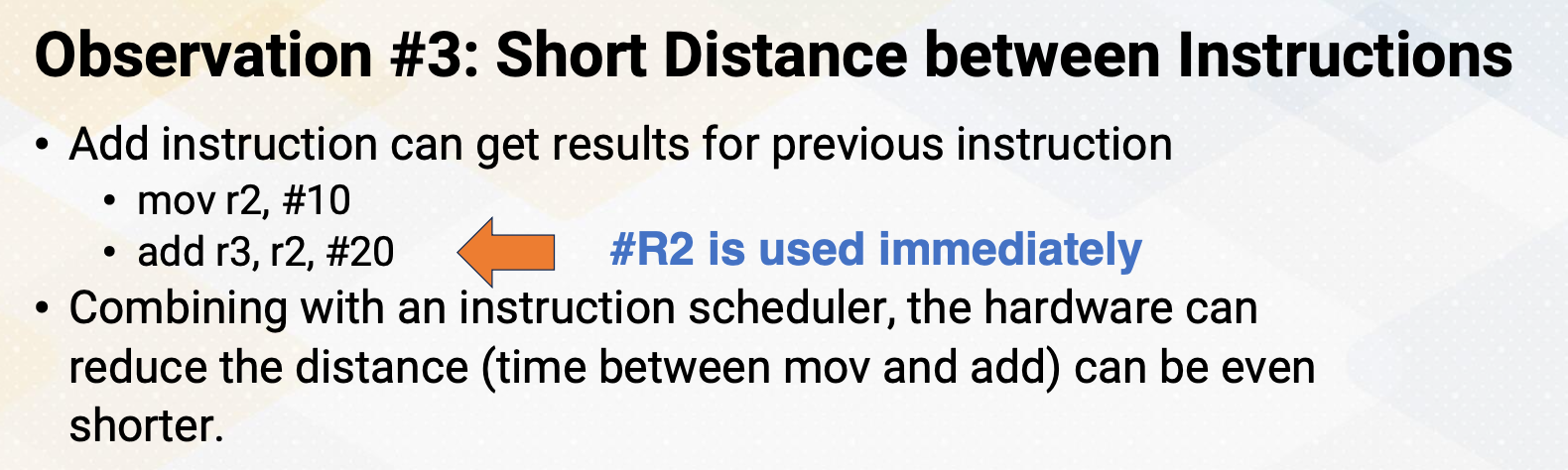
Contrary to just what I described in this slide, sometimes there might be a very short distance between instructions. In a similar example, move instructions store value 10 to r2 register and the subsequent add instruction uses the value of r2 and r2 value will be used immediately. If a scheduler schedules the next instruction immediately after move instruction, then hardware can reduce the time between storing r2 value. So then it also brings a question whether it is necessary to store the value 10 into the register r2.
Observation 4: Most Register Values are Read Only
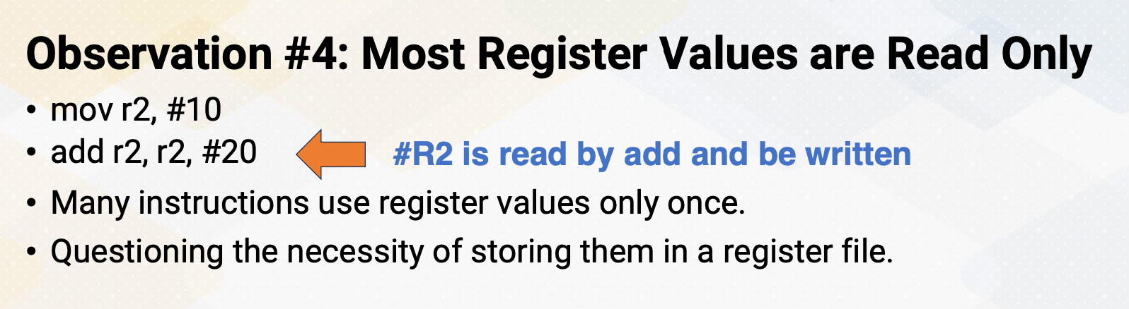
This problem gets even more worse because most register values are read only once. Similar example shows that r2 value has a 10 and then soon after this r2 value will be overwritten after read only once. It was observed that almost 70% of register values are read only once on GPUs. This brings up question whether it is even necessary to store the value into a register file from the beginning, and can you just bypass this register value stores.
Optimization 1: Hierarchical Register Files
Based on these observations, several optimization techniques were proposed.
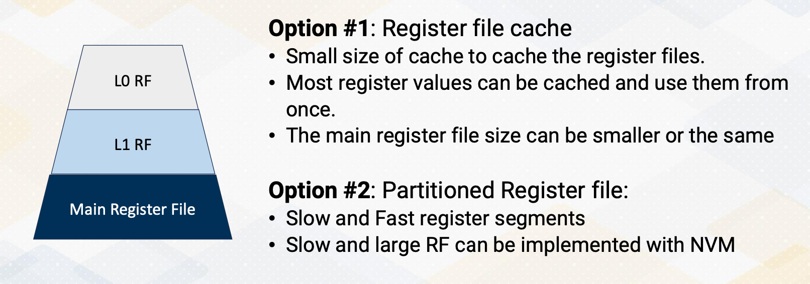
The first optimization technique is using hierarchical register file. In this approach, there are two options to build hierarchical register files. And the first option is utilizing register file cache. Typically, smaller side of structure provides the fast accesses. So smaller side of register file cache can store the value and provide fast accesses. And the main register file size can be even also smaller if we avoid storing all the values into the main register file. Sometimes, the harderware decides to store all the values in that case the main register file size needs to be the same. But regardless of that, by having this hierarchical structure, we can provide fast access to the L0 or L1 register file and have a slow access for the main register file.
This can even optimize further by having partitioned register file. We can use different technology to store slow and fast registers. We can even have using non-volatile memory to store large and slow register file to reduce energy consumptions.
Optimization 2: Register File Virtualizations
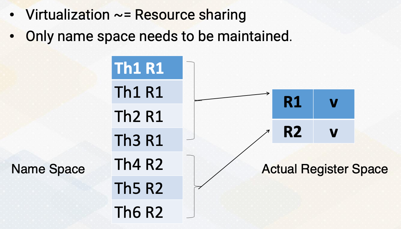
Another approach is to use register file virtualizations. Here we use virtualizations for resource sharing purpose because as we discuss it in the observations, not all registers are actually needed to store the values. So instead of having a register file for every single register items, we can have a small physical register file to store the actual value and only keep the name space by having separate name space and physical register storage, we can still maintain the program characteristics, but we can have very small hardware features.
So in summary in this video, we observed several GPU programming characteristics and have learned several opportunities to optimize for registers. And the main lessons are in several cases, not all registers are actively used. And we also have studied register file optimize techniques to increase the resource sharing and also to improve the latency.
Module 6 Lesson 3: Unified Register File and Shared Memory
Course Learning Objectives:
- Explain optimization opportunities for unified memory and register file
- Differentiate between register files and memory
- Review the concept of occupancy in GPU programming
In this video, we’ll continue GPU architecture optimization techniques by understanding unified register file and shared memory structure. The focus of this video will be to explain optimization opportunities for unified the memory and register file. We will also learn how to differentiate between register file and memory, and we will also review the concept of occupancy in GPU programming.
Review Occupancy
Let’s review the occupancy concept. In cuda programming the resource constraints affect the maximum number of blocks on each streaming multiprocessor (SM). The shared memory requirements or register file size is a critical factor.
For example, in hardware, each SM has 64 kilobyte registers and 32 kilobyte shared memory.
- In the one software example case, each block has 64 registers and no shared memory usages.
- In another software example case each block has four registers and two kilobyte shared memory.
- In Case 1, the shared memory will be underutilized because there is no shared memory usage.
- In Case 2, register file size will be underutilized because at the end, four times number of total cuda blocks and number of threads will be used for the register file size. So in this example will be probably two kilobyte.
So the question is what if we have the shared memory and register file and can we increase the occupancy?
Hardware Cache vs. Software Managed Cache
Before we answer the question, let’s review hardware managed cache, and software managed cache.
- In hardware managed cache hardware decides which memory content will be cached based on LLU or other policies.
- Because not all memory contents will be stored other address tag bits are needed to check whether an address is in the cache or not.
- On the other hand, in software managed cache programmer specifies.
- So address tags are not needed because when the program says it is a software managed cache, that means that content will be inside the memory or inside the cache.
Register File vs. Software Managed Cache
Let’s also review register file and software managed cache. Software managed cache means typically on-chip memory which is very small.
The common characteristics are both are storing data only and both do not need to have a tag to check the address. And in both the location indicates the address. And so we can just go to the particular location and fetch the content. The difference is the number read and the number write ports can be different. Especially register typically access two source operands per instruction, whereas typical memory only access one address.
Another benefit is in register files access patterns are known at static time because these instructions know which registers to access. So there could be more opportunities for the register file even though register file requires more read bandwidth.
Proposed Solution: Unified Structures
The proposed solution is unified structures of shared memory and register file. The benefit is because we are sharing the structure, it could increase occupancy.
- But in order to do that, the critical requirement is high memory bandwidth.
- It should have sufficient port for read and write and
- typically it is used bank structure, but now it needs to have more, even higher bank structures because register and shared memory have different access patterns.
- But this flexible resource sharing allows to reduce resource constraints.
- Now we can consider the summation of register file size and shared memory size can be the constraining factor to decide the occupancy.
So in summary, in this video, we reviewed differences between software managed cache and hardware cache and explored the benefit of unified memory and register file structure. And more kinds of this efficient resource sharing is needed for optimization of GPU performance and power.
Module 7: GPU Architecture Optimizations - II
Objectives
- Describe the performance issues related to divergent branches and the basic mechanisms for handling them.
Readings
Required Reading:
- Power, M. D. Hill, and D. A. Wood, “Supporting x86-64 address translation for 100s of gpu lanes,” in 2014 IEEE 20th International Symposium on High Performance Computer Architecture (HPCA), 2014,pp. 568–578. (https://ieeexplore.ieee.org/document/6835965)
- Narasiman, M. Shebanow, C. J. Lee, R. Miftakhutdinov, O. Mutlu and Y. N. Patt, “Improving GPU performance via large warps and two-level warp scheduling,” 2011 44th Annual IEEE/ACM International Symposium on Microarchitecture (MICRO), Porto Alegre, Brazil, 2011, pp. 308-317.
- T. G. Rogers, M. O’Connor and T. M. Aamodt, “Cache-Conscious Wavefront Scheduling,” 2012 45th Annual IEEE/ACM International Symposium on Microarchitecture, Vancouver, BC, Canada, 2012, pp. 72-83, doi: 10.1109/MICRO.2012.16. keywords: {Benchmark testing;Instruction sets;Graphics processing units;Kernel;Limiting;Registers;Processor scheduling},
Optional Suggested Readings:
- Mark Gebhart, Daniel R. Johnson, David Tarjan, Stephen W. Keckler, William J. Dally, Erik Lindholm, and Kevin Skadron. 2011. Energy-efficient mechanisms for managing thread context in throughput processors. In Proceedings of the 38th annual international symposium on Computer architecture (ISCA ‘11). Association for Computing Machinery, New York, NY, USA, 235–246. https://doi.org/10.1145/2000064.2000093
- Ganguly, D., Zhang, Z., Yang, J., & Melhem, R. (2019). Interplay between hardware prefetcher and page eviction policy in CPU-GPU unified virtual memory. In 2019 ACM/IEEE 46th Annual International Symposium on Computer Architecture (ISCA) (pp. 224-235). Phoenix, AZ.
- Jog, A., Kayiran, O., Nachiappan, N. C., Mishra, A. K., Kandemir, M. T., Mutlu, O., Iyer, R., & Das, C. R. (2013). OWL: Cooperative thread array aware scheduling techniques for improving GPGPU performance. In Proc. of the ACM Architectural Support for Programming Languages and Operating Systems (ASPLOS) 2013 DOI: 10.1145/2451116.2451158
- Jog, A., Kayiran, O., Mishra, A. K., Kandemir, M. T., Mutlu, O., Iyer, R., & Das, C. R. (2013). Orchestrated scheduling and prefetching for GPGPUs. In Proc. of the ACM/IEEE International Symposium on Computer Architecture (ISCA), 2013 DOI: 10.1145/2508148.2485951
- Ausavarungnirun, J. Landgraf, V. Miller, S. Ghose, J. Gandhi, C. J. Rossbach, and O. Mutlu, “Mosaic: A gpu memory manager with application-transparent support for multiple page sizes,” in 2017 50th Annual IEEE/ACM International Symposium on Microarchitecture (MICRO), 2017, pp. 136–150
- Li, J. Yin, Y. Zhang, and X. Tang, “Improving address translation in multi-gpus via sharing and spilling aware tlb design,” in MICRO-54: 54th Annual IEEE/ACM International Symposium on Microarchitecture, ser. MICRO ’21. New York, NY, USA: Association for Computing Machinery, 2021, p. 1154–1168.
- Hyojong Kim, Jaewoong Sim, Prasun Gera, Ramyad Hadidi, and Hyesoon Kim. 2020. Batch-Aware Unified Memory Management in GPUs for Irregular Workloads. In Proceedings of the Twenty-Fifth International Conference on Architectural Support for Programming Languages and Operating Systems (ASPLOS ‘20). Association for Computing Machinery, New York, NY, USA, 1357–1370. https://doi.org/10.1145/3373376.3378529
Module 7 Lesson 1 : GPU Virtual Memory
Course Learning Objectives:
- Explain the concept of GPU virtual memory and its importance in modern GPU architectures
- Explain challenges of GPU address translation, including scalability and handling uncoalesced memory accesses
- Explore hardware optimization opportunities for GPU address translations to improve GPU performance and efficiency
In this video, we will explain the concept of GPU virtual memory and why it is essential in modern GPU architectures. We’ll also discuss the challenges related to the GPU address translation, such as scalability concerns and managed uncoalesced memory accesses. Additionally, we’ll explore opportunities for hardware optimizations in GPU address translations to enhance overall GPU performance and efficiency.
Supporting Virtual Memory
Let’s explore two key aspects of virtual memory: Address translation and page allocations.
- In the CPU, the operating system takes care of page allocations.
- However, in the GPU, the process is slightly different. Initially, the CPU manages the pages in collaboration with the GPU driver. For memory allocation and data management, we rely on functions like cudaMalloc, cudaMallocManaged, and cudaMemcpy.
- These functions are used to allocate memory and facilitate the transfer of managed data.
Review of Address Translations
Let’s review address translation. First, programmers write programs assuming virtual addresses and these virtual addresses need to be mapped to physical addresses. There are several key terms, VPN, virtual page number, PFN, physical frame number, or PPN, physical page number, and PO, page offset.
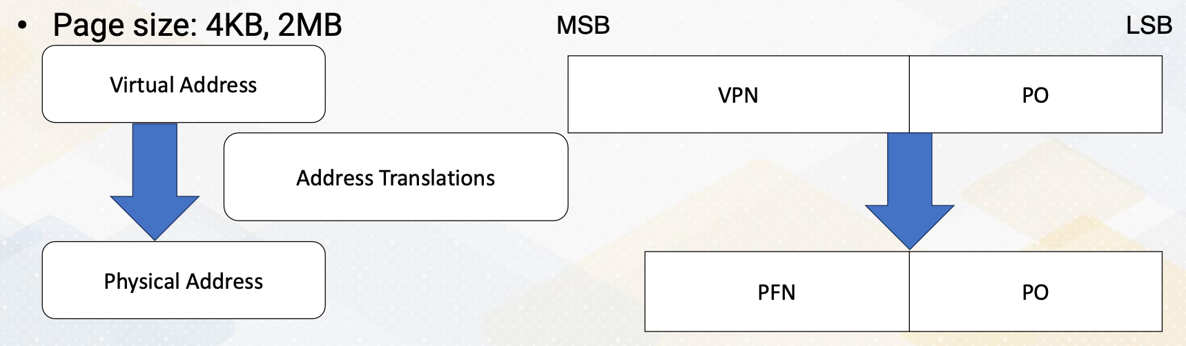
In the address translation, VPN becomes PFN. Page offset stays the same. Typical common page sizes are four kilobyte and two megabyte. Pages are typically divided into fixed size chunks like four kilobyte or two megabyte.
TLB and Page Size
- TLB as a translation look-aside buffer, is a cache to store address translation. TLB stores recently used address translation to speed up future accesses.
- Page table entry, PTE, stores mapping from VPN to PFN. PTE itself is the memory, So accessing PTE itself requires multiple memory accesses, hence TLB caches PTE so that it can avoid multiple memory accesses for PTE.
- TLB miss requires a page table access to retrieve address translation. If an address isn’t found in the TLB, the page table must be accessed, which takes more time.
- Page fault occurs when no physical page is mapped yet, and then OS needs to allocate a page.
4 Level Address Translation
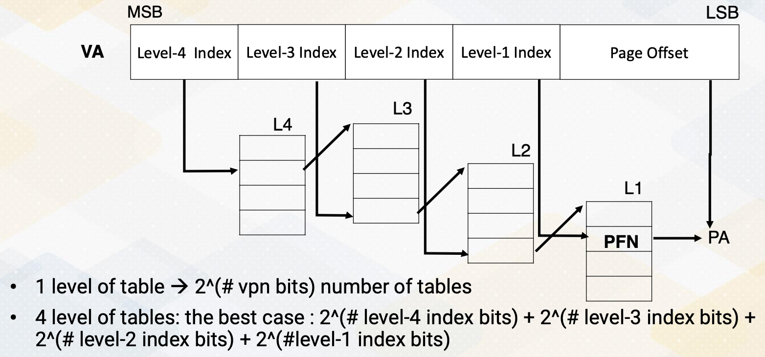
Here is an example of four level address translation. Similar structures are used in x86, ARM, and even GPUs. The reason we have four levels is that if we didn’t have any levels, the number of table entries would be equal to 2 to the power of the number of VPN bits, which is 2 to the 48th power. All the tables would need to be stored in memory, result in a massive number of entries. Hence, we use multi-level tables. When we use multiple levels, we don’t have to store all the tables. The best case scenario would be 2 to the power of level 4 index bits, which is 12 bits, plus 2 to the power of the number of level 3 index bits, plus 2 to the power of the number of level 2 index bits, and finally, 2 to the power of the number of level 1 index bit.
This results in thousands of entries as opposed to a trillion number of entries. The downside is that address translation needs to traverse through multiple levels of tables. First, it use sthe level 4 index to access the level 4 table and within the table entry, you will find the starting address of the corresponding table 3 entry. Then using the level 3 index bit, it accesses an entry in the level 3 table, which in turn provides a corresponding level 2 starting address. Continuing with the level 2 index bit, index table giving you the starting address of the level 1 table. This process repeats until you reach the level 1 entry which finally stores the PTE containing the PFN number and other metadata. Using the PFN and page offset, the system can compute the physical address.
Hence, with 4 level address translation, a single address translation requires at least four memory accesses. This process is often referred to as a walk. Address translation can be performed by hardware through a hardware page table walker, which is called PTW, or by software.
Virtual Memory on GPUs
Now let’s discuss GPU virtual memory.
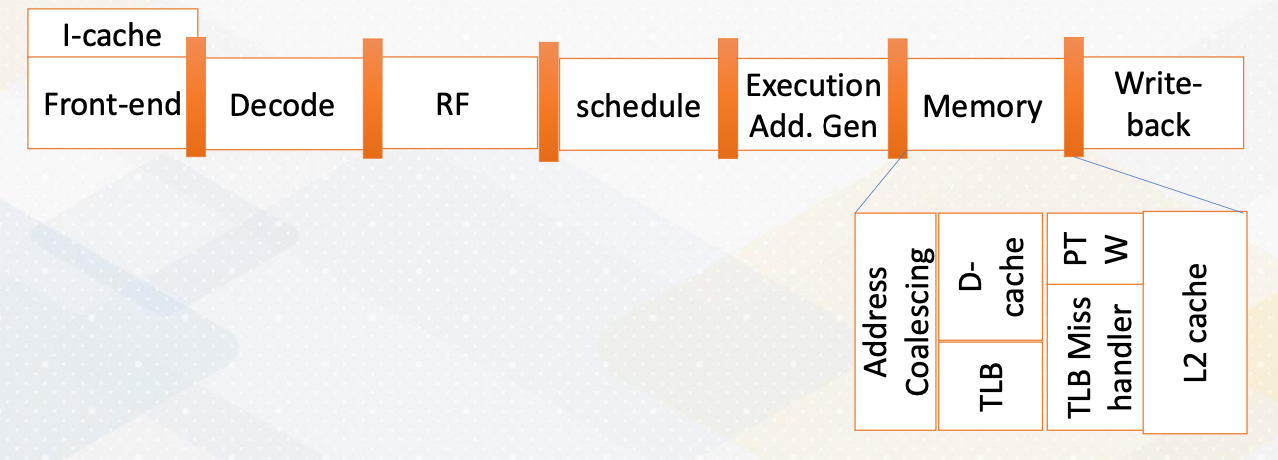
- In earlier GPUs, there was no virtual memory or it has only on-to-one mapping.
- As GPUs have become more programmable, the need for complex memory system support has risen such as unified virtual address.
- Address translation shares similar mechanisms with the CPUs except for address coalescing.
The memory address stage is divided into address coalescing and TLB accesses. If a TLB miss occurs, the page table walker retrieves a new page table entry or the TLB miss handler manages the TLB misses. Typically, L1 cache accesses use virtual memory addresses, while L2 cache accesses use physical memory accesses.
Memory Coalescing and TLB Accesses
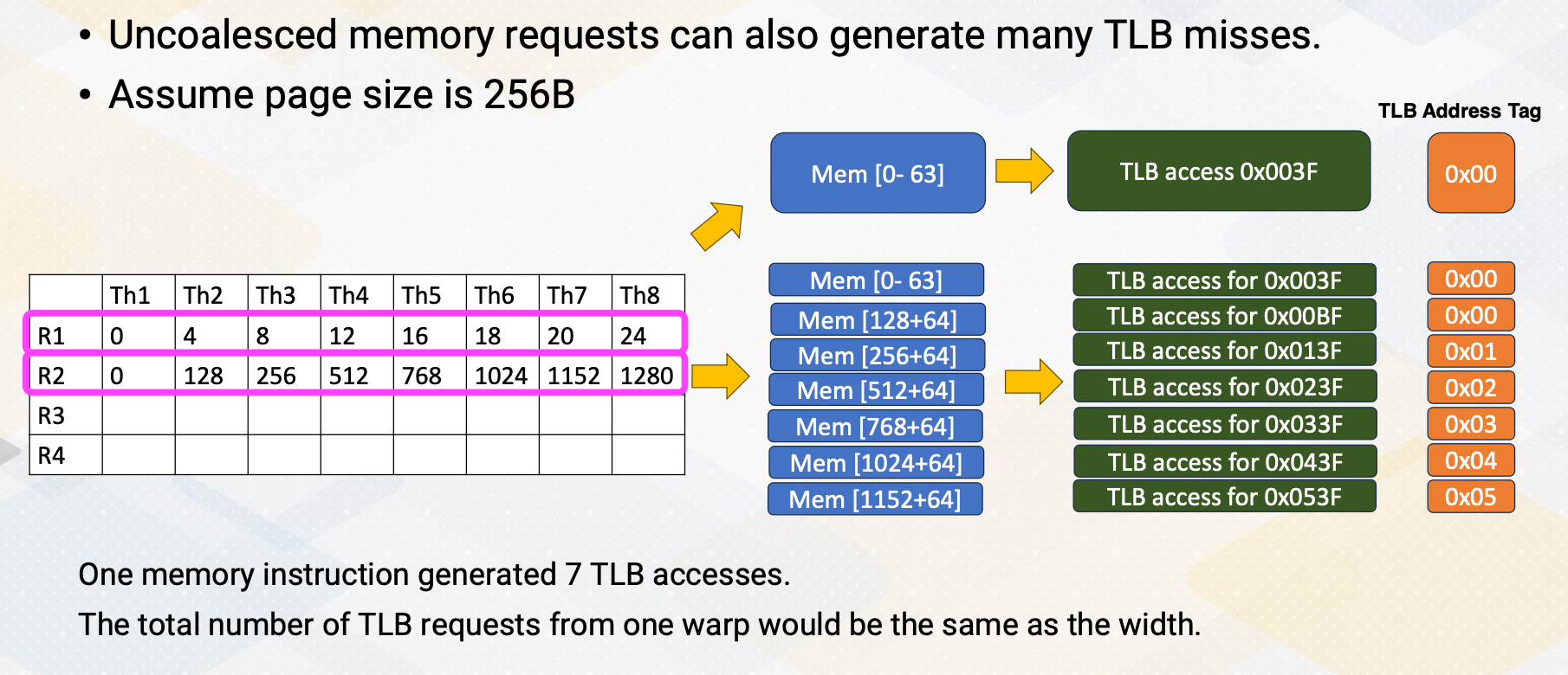
Let’s consider an example where we assume a page size of 256 byte. In the previous example, the first load which is using R1 generate one memory request which result in one TLB access. Similarly, the next load generates only one TLB access with tag 0X00. In the second example, multiple memory requests (eight of them) are generated, but they won’t be coalesced. Each of them generate separate TLB accesses. If we examine the TLB address tags, the first two addresses are actually combined into one TLB access, but the rest are separate TLB accesses. Therefore, one memory instruction ends up generating seven TLB accesses. In uncoalesced memory accesses, the total number of TLB requests from one warp would be the same as the number of width of a warp.
Challenges of GPU Address Translation
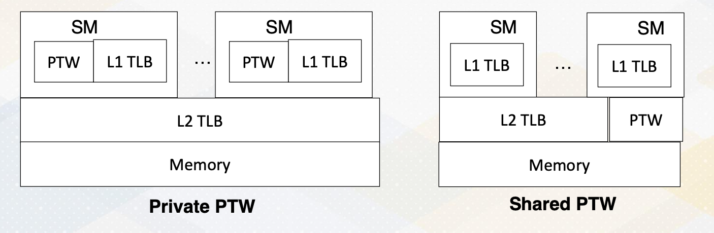
The challenge in GPU address translation lies in achieving scalability. A single warp TLB miss can lead to the generation of multiple TLB misses, particularly in case of uncoalesced memory accesses. Hence, the critical factor is having high bandwidth of the PTW, and one option is sharing a high bandwidth PTW across multiple SMs.
Techniques to Reduce Address Translation Cost
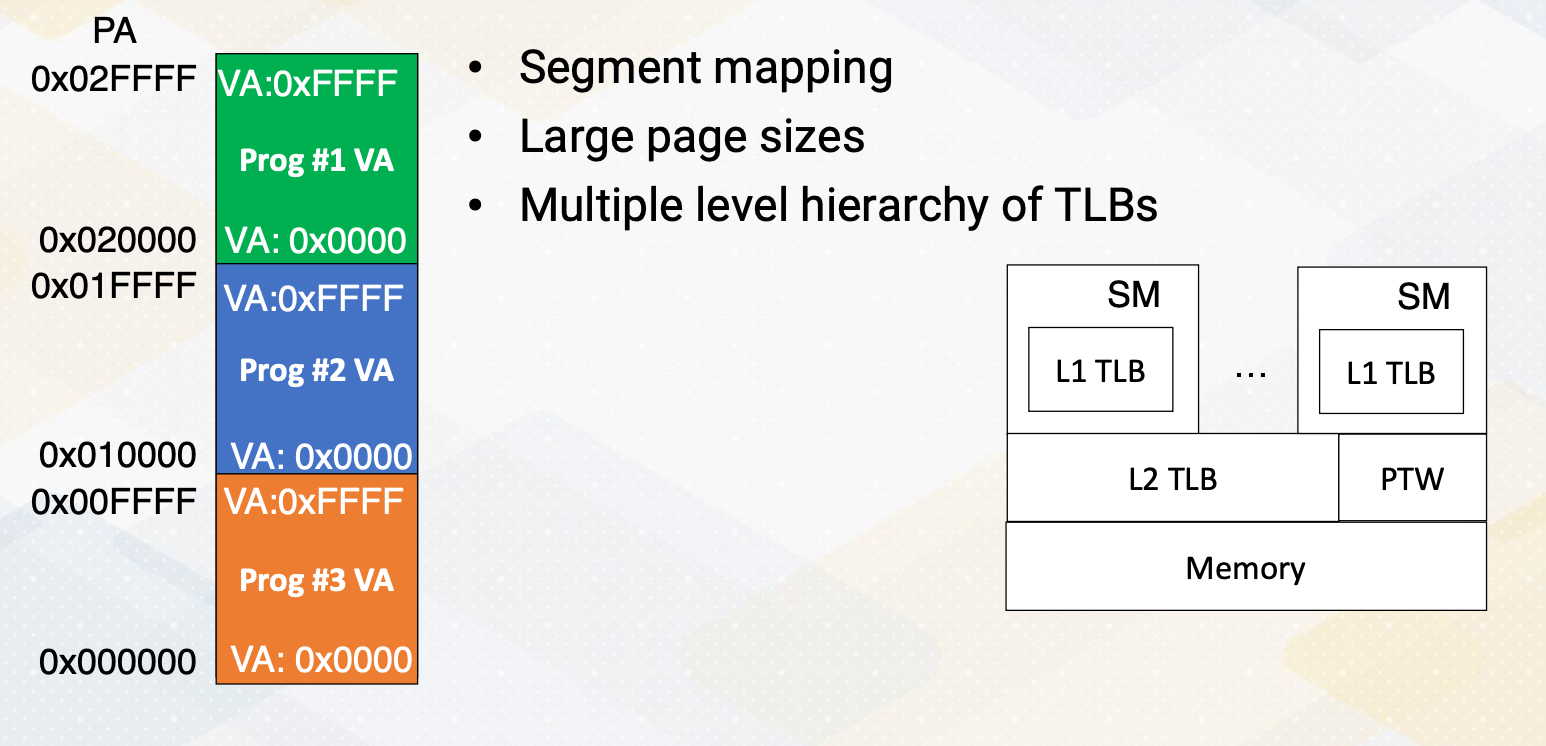
Let’s discuss techniques to reduce address translation cost, which can include segment mapping, large page sizes, and the concept of multiple levels in TLB hierarchies. In segment mapping, each virtual address space corresponds to a portion of the physical address space. For instance, each program requires the address space from 0x0000 to 0xFFFF. We assign the orange area, 0x000000, to 0x00FFFF to program 3, and the blue area to program 2, and the green area to program 1. With this arrangement, during address translation, we can simply add the upper 2 bits (0,1, or 2) to access physical addresses result in very low cost address translation. The figure on the right slide illustrates two levels of TLB hierarchies.
Large Pages
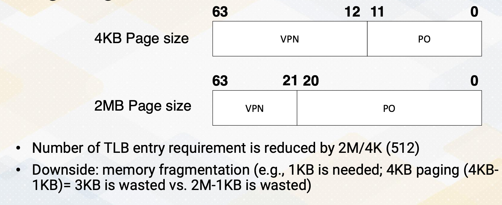
Typical page sizes is four kilobyte with two megabyte pages. And in this case, the number of VPN is reduced from 51 bits to 42 bits. The number of TLB entries also reduced by 512. However, there is a downside to this approach, which is memory fragmentation. For example, if only one kilobyte of memory is needed, the system uses four kilobyte paging, it wastes three kilobyte of memory. This contrasts with the case when you use two megabyte memory system, it wastes 2 megabyte minus 1 kilobyte. In summary, memory address coalescing plays a critical role in address translation. Furthermore, ensuring scalable address translation is most important, which includes aspects like resource sharing and the use of large pages.
Module 7 Lesson 2 : GPU Virtual Memory - UVA
Course Learning Objectives:
- Explain Unified Virtual Address Space (UVA)
- Explore challenges associated with on-demand page allocations
In this video we’ll continue study GPU virtual memory. By the end of this video you should be able to explain Unified Virtual Address Space, UVA, and you should be able to explore challenges associated with on-demand page allocations.
Review: Global Memory Management
Let’s review the host code of cuda. We can see three API calls, cudaMalloc and cudaMemcpy. Here cudaMalloc allocates memory in the GPU and cudaMemcpy transfers data between CPU and GPU.
GPU Memory Page Allocations
Let’s discuss deeper into GPU page allocations.
- In earlier GPUs they followed the copy then execute model. This model involves copying data from the CPU to the GPU before executing a kernel.
- It utilizes functions like cudaMalloc for GPU memory allocation and cudaMemcpy for data transfers. This ensures that all necessary data is available on the GPU for computation. This implies explicit data transfer.
- Data must be explicitly moved between the CPU and GPU before launching a kernel.
- The benefit includes efficient PCI-E bandwidth usage, allowing programmers to optimize PCI-E bandwidth.
- It’s a part of pre-kernel preparation where GPU drivers set up and data management occur before kernel execution.
- The downside of explicit page management is that it requires programmers to manually manage memory pages which can be complex.
Unified Virtual Address Space (UVA)
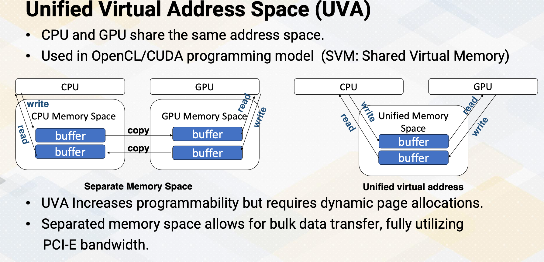
Unified Virtual Address space. In UVA, CPU and GPU share the same address space. This approach is commonly used in the OpenCL/CUDA programming model and is known as SVM, Shared Virtual Memory. UVA increases programmability. SVM enhances programmability by allowing both the CPU and GPU to operate within the same address space. However, this approach requires dynamic page allocation to manage memory efficiently.
On the other hand, the separated memory space permits efficient bulk data transfer, making full use of PCI-E bandwidth. This is illustrated in the left figure. Logically there are two buffers, one for CPUs and one for GPUs. In the case UVA, logically there is only one buffer and it can be accessed by both CPUs and GPUs. For separate memory space, logically CPU writes only to CPU buffer and GPU writes into only GPU buffer and then there needs to be explicit copy.
Page Fault Handling Path
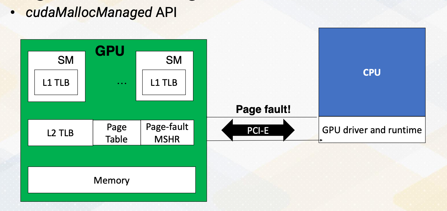
However in the UVA, those explicit copy are not needed. However, most GPUs are discrete GPUs in the modern high performance computing which has a separate physical memory system. To support UVA in a discrete GPU set up there needs to be a copy between CPU memory and GPU memory, which involves dynamic memory management. The cudaMallocManaged API handles this and this is also called on-demand memory management. The GPU generates a page default and the request needed to be sent to the CPU. The CPU’s operating system and GPU’s driver handles this page fault and then send the information back to the GPU. Consequently, the latency can be in the range of tens of milliseconds.
Background: IOMMU
Let me briefly provide a background on IOMMU.
- IOMMU, which stands for input-output memory management unit,
- serves as a bridge between input-output devices and the memory management unit. Its primary function is to enable direct memory accesses, DMA accesses, using virtual addresses.
- This means that it allows for I/O virtualization by utilizing virtual addresses for DMA operations instead of physical addresses.
- Both the CPU and GPU are equipped with their own IOMMUs. In the case of GPU, each virtual page management is seamlessly integrated into this unit.
Previously, GPU memory was solely managed by IOMMU, as GPU memory was treated as peripheral devices. However, with the UVA, not only the IOMMU, but also the CPU actively involves in the management.
Challenges of On-Demand GPU Memory
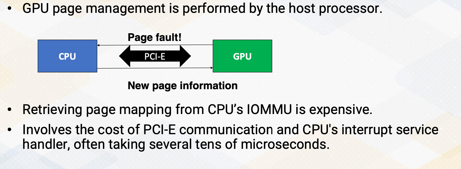
What are the challenges of on-demand GPU memory, which is crucial for UVA? GPU page management is performed by the host processor. Retrieving page mapping from the CPU’s IOMMU can be costly, involving the overhead of PCI-E communication and the CPU’s interrupt service handler. This process often takes several tens of microseconds.
Techniques to Reduce the Overhead OnDemand
Certain techniques can help reduce overhead of on-demand memory allocation. For instance, we can employ techniques like on-demand or prefetching of pages to predict future memory addresses and bring them in advance. Another approach is shift page mapping measurement to the GPU side instead of CPUs. Additionally, cooperative effort between CPU and GPU driver can be beneficial, with the CPU handling large memory chunk while the GPU manages small pages within the same large chunk.
Background of Memory Prefetching
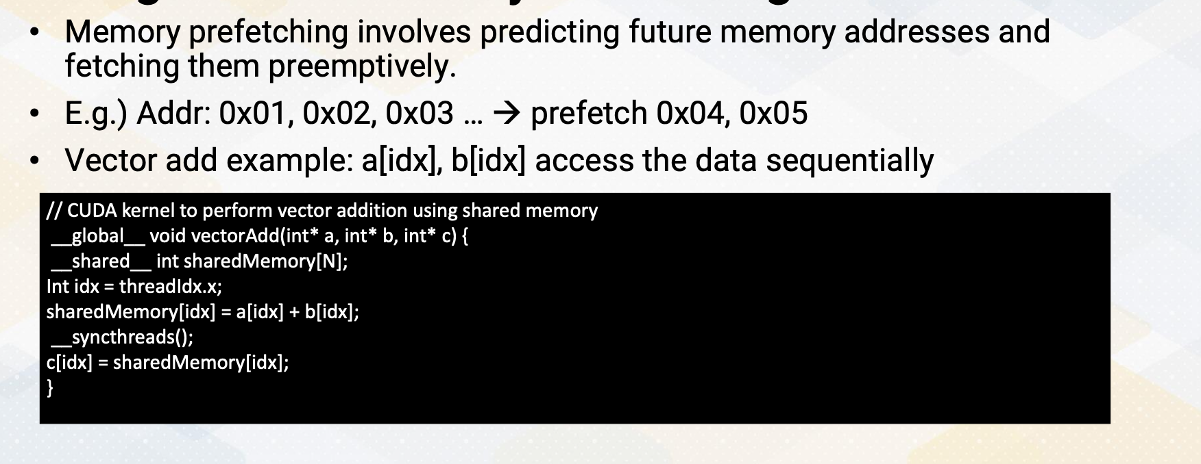
Let’s look at the background of memory prefetching. Memory prefetching is a technique that involves predicting future memory accesses and fetching them in advance. For example, if we have a sequence of memory addresses like 0x01-3, the prefetching mechanism would preemptively fetch the next addresses such as 0x04 and 5. To illustrate this concept, consider the example of vector addition and the cuda version of the code is shown here. When accessing element in array a and b using index idx, these accesses are typically done sequentially. Therefore, array a and b are good candidates for prefetching.
Page Prefetching
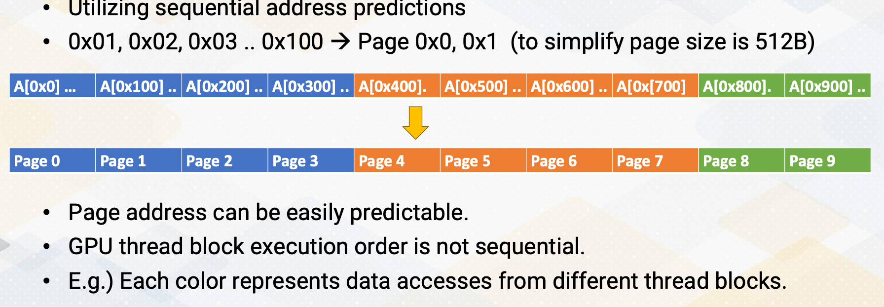
Similar to memory address prefetching, we can also apply this concept to page prefetching. This involves using sequential address predictions such as 0x01-3 and so on to 0x100. To simplify the example, a page size is again 512 byte instead of 4 kilobyte. Here, page addresses can often be easily predictable as shown in this illustration. So we can prefetch pages 1, 2, 3 and so on. However, it is important to note that the execution order of GPU thread block is not necessarily sequential. For example, in the illustration here each color represents data accesses from different thread blocks, highlighting their concurrent and non-sequential execution.
Tree-Based Neighborhood Prefetching
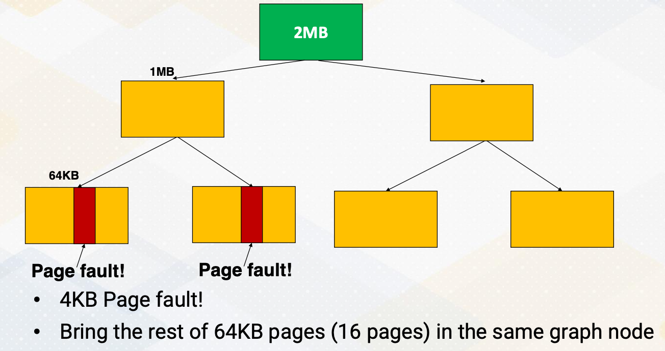
To address this issue of out of order execution of thread blocks, NVIDIA employs a tree-based neighborhood prefetching approach. Initially, it divides a 2 megabyte chunk into two 1 megabyte sections, then it creates 64 kilobyte nodes within these sections. If a page fault occurs within a node, the system fetches entire 64 kilobyte. Another node, if there is a page fault, it fetches all 64 kilobyte again. If multiple nodes generate prefetch request, it fetches the upper node of page which becomes 1 megabyte. This way it detects spatial locality but also limits the size of prefetched blocks.
GPU Memory Oversubscription
GPU memory oversubscription. It becomes an issue when allocating an excessive amount of virtual memory space to GPUs. This situation often leads to page eviction as there are not enough pages to accommodate the demand memory request. The question then arises, which pages should be evicted? Prefetching plays a critical role in addressing these challenges. As the demand on GPU kernel memory continues to increase, the problem of GPU memory oversubscriptions becomes even more pressing. In summary, this video highlights several challenges in Unified Virtual Address space, UVA, management and underscores the importance of employing page prefetching techniques to tackle these challenges. It also touches upon the comparisons between on-demand memory allocations and the copy and execute model.
Module 7 Lesson 3 : GPU Warp Scheduling
Course Learning Objectives:
- Explain the fundamentals of GPU warp scheduling policies
- Explore the challenges and considerations involved in GPU warp scheduling
- Explain Round-Robin, GTO and other scheduling policies
In this video, we’ll discuss GPU Warp Scheduling. Our learning objectives for this video include gaining a solid understanding of GPU warp scheduling policies, we will explore the various challenges and considerations that come into play when it comes to GPU warp scheduling. Additionally, we’ll explore different scheduling policies including Round-Robin and GTO to get a comprehensive view of this topic.
Review: GPU Pipeline
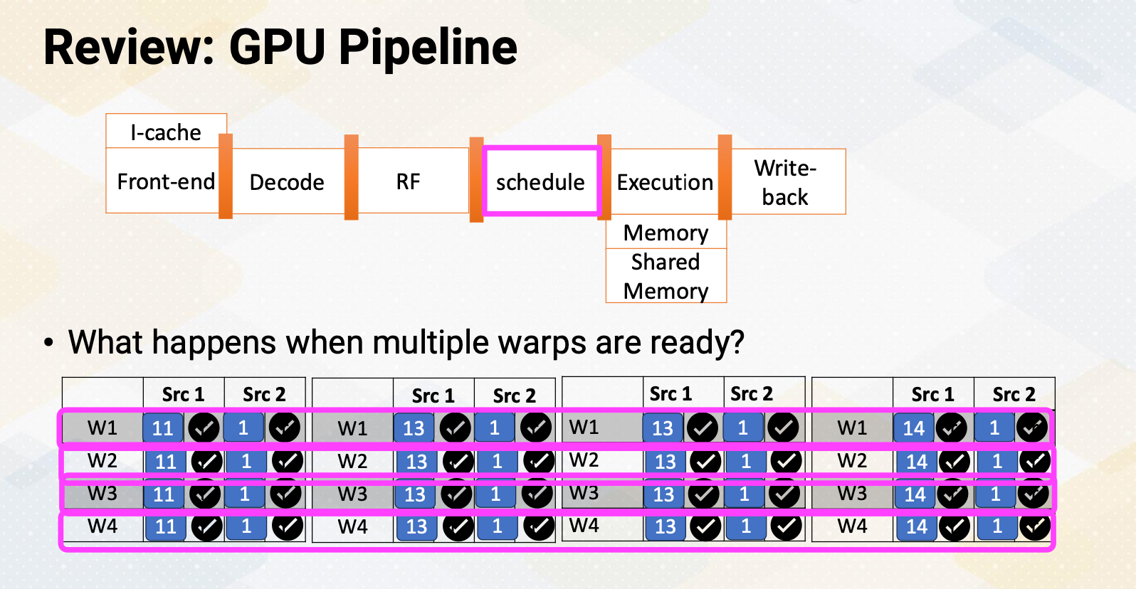
We discussed GPU pipeline before which is fetch, decode, register file access, and scheduler and so on. So far we discussed as if there is only one warp ready to be scheduled at a time. But what if there are multiple warps that are ready? Like in this example there are four warps that are ready which you want to choose to schedule. This is a warp scheduler’s job.
CPU Instruction Scheduler
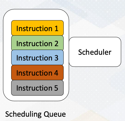
Let’s begin by discussing the CPU instruction scheduler. In the context of CPU instruction scheduling, it selects from the available ready instructions. This process involves examining all instructions in the scheduler especially those that cannot be divided into multiple cycles. Within CPU instruction scheduling, several policies come into play including oldest first critical instruction first. And as an example of critical instruction first, there are load instructions first and instruction with many dependent instructions first.
For example, load instruction first policy it proves usefulness in generating memory requests as soon as the load address becomes ready. Additionally, prioritizing instructions with many dependent instructions can lead to other dependent instructions become ready sooner.
GPU Warp Scheduler
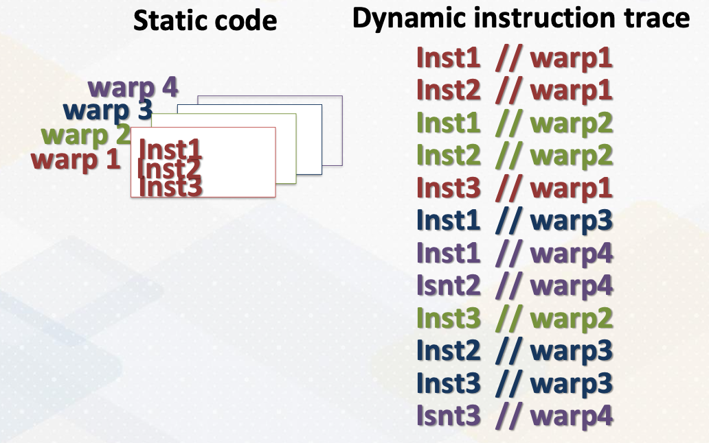
The GPU warp scheduler implements an in-order scheduler. However, even though it’s an in-order scheduler, when there are multiple warps ready, it selects and executes whichever warp is ready. Hence if you examine the final execution of instruction stream, they all appear to be out of order execution.
RR vs GTO
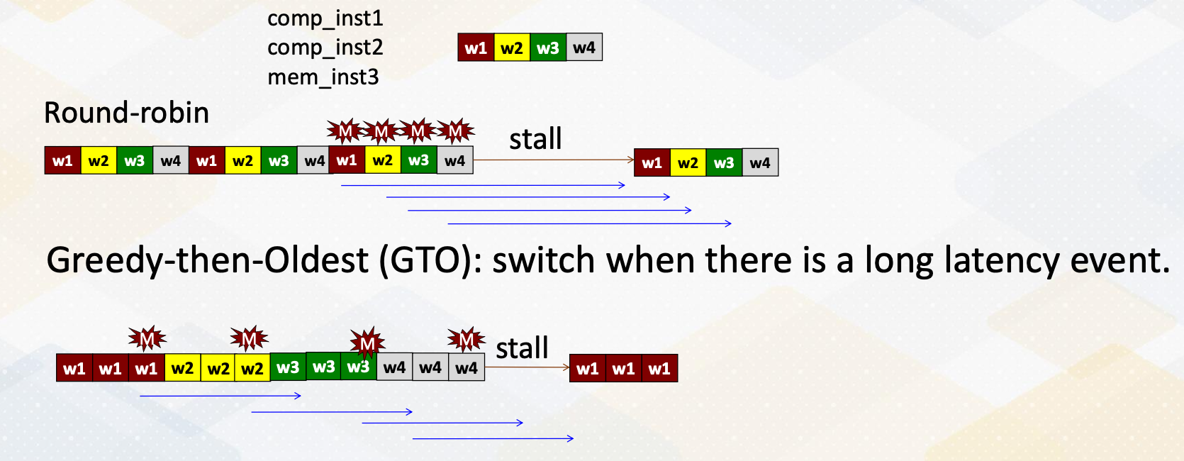
Let’s discuss the two most basic GPU warp scheduling policies which are Round-Robin and GTO greedy-then-oldest. In this example, there are three instructions each represented by a different color for different warps. In the Round-Robin, it selects one instruction from one warp in a Round-Robin fashion like this. The third instruction which is a memory instruction generate cache miss and then switch it to another warp and so forth. Hence, all four memory requests are generated almost simultaneously. Therefore the latency cannot be hidden so the pipeline has a stall and once the first memory request from the warp 1 returns, it resumes execution and then continues.
On the other hand, GTO starts with only one warp initially, the oldest one, and then it switches to another one when there is a long latency event such as a cache miss, branches or lengthy tensor core operations. In this example the memory address generates a long event, and whenever there is a cache miss is switches to another warp 1,2,3 and then 4th. In this case, it actually generates memory request from the first warp early enough to reduce the overall stall cycles but benefit depending on the specific program characteristics.
Two-Level Scheduling
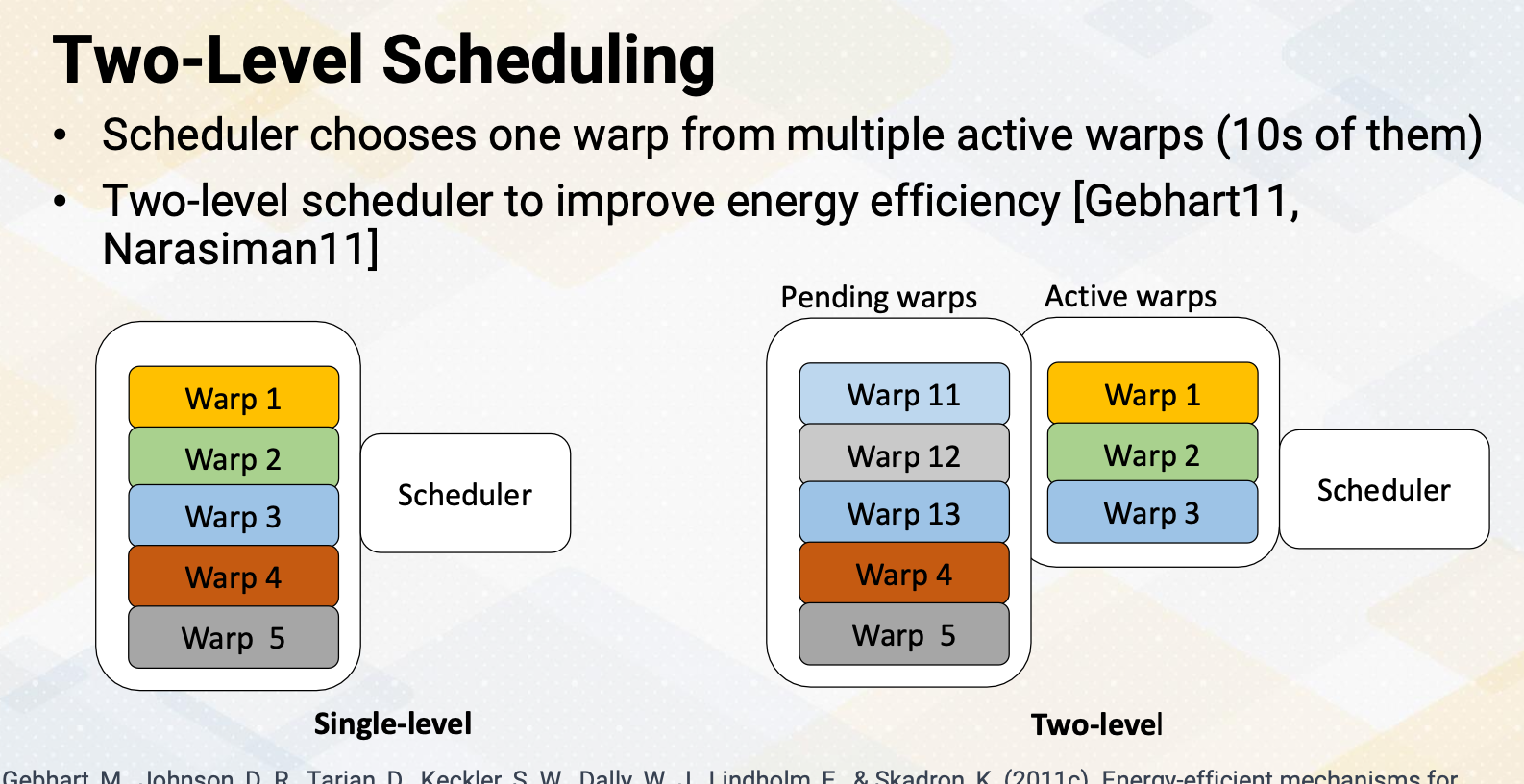
The challenge for the scheduler is that it has to probe to determine which instructions are ready. The task actually consumes a significant amount of power. Hence in a single level scheduler, it needs to search the entire scheduler queue just to schedule only one instruction. To reduce this inefficiency, a two-level scheduler was proposed. In the two- level scheduler, the warps are divided into two groups, pending warps and active warps. The scheduler only searches the active warps queue and choose one from there.
Warp Scheduling and Cache Behavior
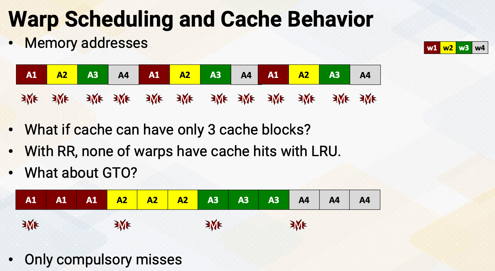
Another interesting aspect of the wrap scheduler is impact on cache behavior. Let’s assume there are four warps and each warp repetitively accesses the memory addresses A1, A2, A3, and A4. The diagram illustrates the Round-Robin scheduling policy and the memory addresses. Suppose there is a cache but it can only accommodate three blocks. Due to the LRU replacement policy when the 4th warp accessed A4 it evicts A1. When A1 is needed again it results in a cache miss and evicts A2 but insert A1. This pattern continues result in cache misses for all blocks. Now let’s consider the GTO scheduling policy. It brings A1 and A1 remains in the cache. When it’s time to start warp 2, it brings A2 and insert into the cache. Again, A2 will be in the cache for the rest of the warp execution. This repeats for all four warps. Hence in the GTO scheduling policy, only compulsory misses occur which is an ideal scenario.
Warp Scheduler and Working Set Size
The important part is that the warp scheduler’s decision can have an impact on the working set size of the L1 cache. To make this previous example more formal, let’s assume if each warp’s working set size is SS_W and there are N warps in an SM, the working set size for Round-Robin scheduling policy will be SS_W $\times$ N. However, if we limit the number of schedular warps to SW then it would be SS_W $\times$ SW. It is important to note that in the case of GTO, SW may not necessarily be equal to one. As GTO may schedule to another warp in the event of a long latency instruction.
Cache Conscious Scheduling Policy (Roger 12)
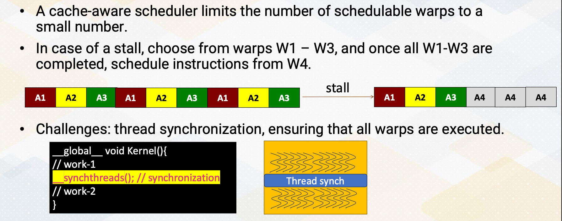
A cache aware scheduler limits the number of schedulable warps to a small quantity. In the GTO when encountering a stall it selects warps from warp 1-3 and then it switches to another warp. However in the cache aware scheduler it selects instruction from warp 1-3 and once they are completed it processes to schedule instruction from warp 4. The challenge lies in case where a program involves thread synchronization and it must ensure that all warps are executed. Another challenge is determining the appropriate number of active warps to schedule. In general, having more warps increase parallelism. However, by limiting the number of warps, it might reduce the cache working set sizes but it also restricts warp level parallesm. Consequently depending on the cache behavior and program characteristics, the optimal number of active warps needs to be selected.
Other Warp Scheduling Polices
Here are some other warp scheduling policies. We have the prefetching aware warp scheduler which is built upon the two-level scheduler as discussed in Jog’s work. The scheduler operates on the concept of fetching data from non-consecutive warps with the goal of enhancing bank-level parallelism. Another approach is a CTA-Aware Scheduling also presented by Jog. CTA-Aware scheduling takes into account the characteristics of Cooperative Thread Arrays and provide control over which CTAs are scheduled. In summary, we’ve covered scheduling policies like Round-Robin and Greedy-the- oldest. We learned that implementing a 2-level warp scheduler can lead to substantial energy savings. The warp scheduler’s choices can influence the effective working set size with a cache conscious scheduling policy being one example. Additionally, we’ve explored various other opportunities for scheduling optimizations.
Module 8: GPU Simulation
Objectives
- Gain an understanding of the fundamental concepts required for modeling GPU architecture simulations.
- Learn how to employ analytical models for performance modeling of GPUs.
Readings
Required Readings:
- Changxi Liu, Yifan Sun, and Trevor E. Carlson. 2023. Photon: A Fine-grained Sampled Simulation Methodology for GPU Workloads. In Proceedings of the 56th Annual IEEE/ACM International Symposium on Microarchitecture (MICRO ‘23). Association for Computing Machinery, New York, NY, USA, 1227–1241. https://doi.org/10.1145/3613424.3623773. (https://dl.acm.org/doi/10.1145/3613424.3623773)
- Samuel Williams, Andrew Waterman, and David Patterson. 2009. Roofline: an insightful visual performance model for multicore architectures. Commun. ACM 52, 4 (April 2009), 65–76. https://doi.org/10.1145/1498765.1498785
Optional Readings
- Computer Architecture Performance Evaluation Methods (Synthesis Lectures on Computer Architecture)https://link.springer.com/book/10.1007/978-3-031-01727-8 (local copy: https://gatech.instructure.com/files/49589403/download?download_frd=1)
- S. Karkhanis and J. E. Smith, “A first-order superscalar processor model,” Proceedings. 31st Annual International Symposium on Computer Architecture, 2004., Munich, Germany, 2004, pp. 338-349, doi: 10.1109/ISCA.2004.1310786.
- Jen-Cheng Huang, Joo Hwan Lee, Hyesoon Kim, and Hsien-Hsin S. Lee. 2014. GPUMech: GPU Performance Modeling Technique Based on Interval Analysis. In Proceedings of the 47th Annual IEEE/ACM International Symposium on Microarchitecture (MICRO-47). IEEE Computer Society, USA, 268–279. https://doi.org/10.1109/MICRO.2014.59
- Sunpyo Hong and Hyesoon Kim. 2009. An analytical model for a GPU architecture with memory-level and thread-level parallelism awareness. In Proceedings of the 36th annual international symposium on Computer architecture (ISCA ‘09). Association for Computing Machinery, New York, NY, USA, 152–163. https://doi.org/10.1145/1555754.1555775Links to an external site.
Module 8 Lesson 1 : GPU Cycle Level Simulation (Part 1)
Course Learning Objectives:
- Describe cycle-level performance modeling for CPUs and GPUs
- Explain queue-based performance modeling
- Describe the basic simulation code structures for CPUs and GPUs
- Get ready for the architecture modeling programming project
Performance Modeling Techniques
There are several performance modeling techniques:
- cycle-level simulation,
- event-driven simulation,
- analytical model,
- sampling-based techniques,
- database statistical and ML modeling, and
- FPGA based emulation.
We will provide a brief introduction of these techniques.
Cycle Level Simulation
- First cycle-level simulation, this is commonly used in many architecture simulators, especially for the earlier hardware design time.
- In the cycle-level simulation, a global clock exists.
- In each cycle, events such as instruction fetch and decode are modeled.
- Multiple clock domains can exist, like memory clock, processor clock, NoC clock domains.
Execution Driven vs. Trace Driven Simulation
In the cycle-level simulation, two types of simulation techniques exist, execution driven versus trace driven. In the execution driven, instructions are executed during the simulation. Depending on when an instruction is actually executed inside the simulator, there are also two different simulators, execute-at-fetch versus execute-at-execute. Execute-at-fetch means instructions are executed when an instruction is fetcheted. Execute-at-execute means instructions are executed at the execution stage. Most of the time this difference is not noticeable, but as execution driven simulator designers, this decision has to be made.
Trace driven is based on traces Here because traces are collected in advance, simulations and executions are decoupled. Benefits of execution driven is there is no need to store traces, and it can also model behavior that vary at runtime. On the other hand, trace driven cannot model run-time dependent behavior such as lock acquire, and barriers. In general, trace driven simulators are simpler and often lighter. So it’s easier to develop. Also, you can just collect memory traces only for memory simulations or cache simulations.
Queue Based Modeling
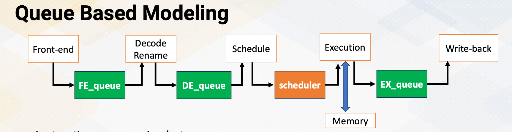
In the cycle-level simulations, queue-based modeling is often used. In the five-stage pipeline between pipeline stages, we’ll have queues except for scheduler. In this diagram, green box shows the queues, and this illustrates how we model five-stage pipeline using queues. Instructions move between queues. Scheduler selects instructions that will be sent to the execution stage among ready instructions. Hence, it is not implemented as a queue structure. Other queues are FIFO structures. When the instruction is complete, the dependent instructions are ready. The dependency chain needs to be modeled and broadcasting also needs to be modeled, just like the actual hardware. Cache and memory are modeled to provide memory instruction latency. Execution latency can be a simple look up table to find the latency if the latency does not depend on runtime behavior.
Modeling Parameters with Queue Based Modeling
Then let’s discuss how to set the modeling parameters when you use queue based modeling. The number of cycles in each pipeline stage is simply modeled by the depth of the queue. How many instructions can move between queues represent pipeline width, such as issue/execution bandwidth. At this moment, you might wonder how we should know the latency of each instruction that we can model. You might wonder whether we need circuit level simulators to find the latency. The answer is we don’t need to measure the instruction latency, instruction latency is given as a parameter such as ADD instruction takes one cycle and MUL instruction takes three cycles. Latencies can be obtained from literature, or we could use more detailed simulators like CACTI or RTL. There are many public documentations that discuss such instruction latency.
5-stage CPU Processor Modeling
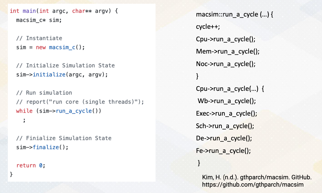
Here is an example of five-stage processor modeling code, which is from a macsim, a CPU and GPU simulator that is developed from Georgia Tech. In the main function, it instantiates macsim simulator. In the simulator, first, it initializes the parameters. After that it starts to call run a cycle of the simulator until the simulation can end. Inside the macsim module’s run a cycle , it increments cycles. Then it goes through CPU memory Noc run a cycle. In the CPU run a cycle, it goes through each pipeline’s run a cycle. The simulator is also built on hierarchical modules.
example
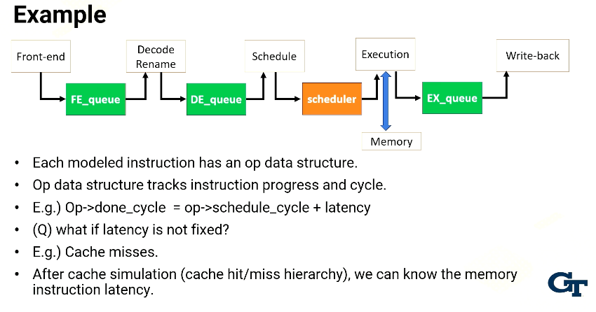
Each modeled instruction has an op data structure. The op structure will go through the pipeline from the front end to the decode stage to the scheduler, execution and write-back and then retires. This op data structure tracks instruction progress and cycles. For example, done_cycle in op data structure indicates the done_cycle by adding schedule time and instruction latency. Done cycle indicates when an instruction is completed. When the processor schedules an instruction, at that time we can know when the instruction is completed if the instruction has a fixed instruction latency. So when the scheduler is executed, it can compute this done cycle. The exception is if the latency is not fixed, such as cache misses. in that case, we use cache simulations which model cache hit and misses. Then we can know the memory instruction latency. And based on those instructions, we add the latency into the done cycle.
Scheduler
The role of scheduler is to identify ready instructions. Scheduler also needs to handle research constraints. For example, even though there are multiple instructions already, this should schedule only the instruction that can be executed for the given resource. For example, number of floating point instructions, number of load and store queues, execution with ports in the cache systems. If an instruction takes multiple cycles, the resource contention should be also considered that. It should ensure that resources are available for multiple cycles.
GPU Cycle-Level Modeling
Now let’s talk about how to model GPU cycle-level modeling. In some sense it is similar to CPU modeling. One of the biggest factor is the simulation execution unit is a warp instead of thread to model SIMT behavior. Warp instruction is model for fetch, decode, schedule, and execution. Scheduler chooses instructions from the head of each warp because it is an in order scheduler. The difference from CPUs is an in order scheduling within a warp, but it can be an out-of-order execution across warps. Major differences between CPU and GPU in terms of modeling are first handling divergent warps. Then warp, thread block, kernel concepts should be implemented to reflect GPU execution model. Scheduler also needs to be modeled significantly differently.
End of Simulation
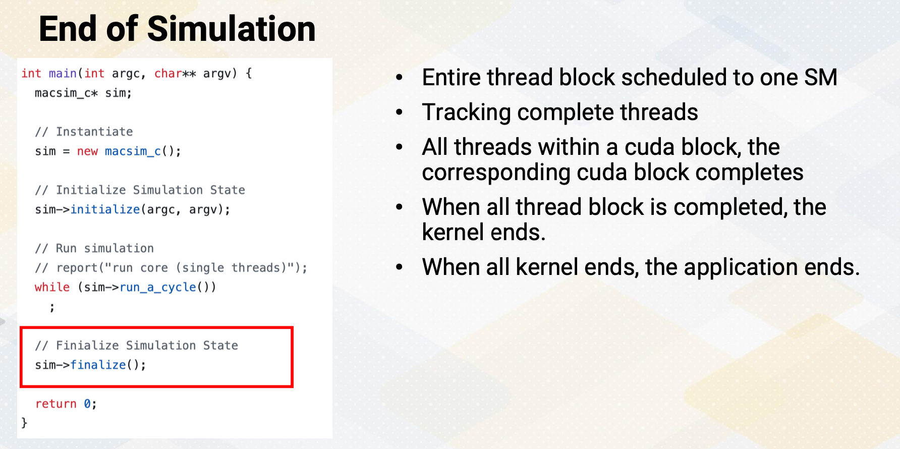
Now let’s discuss the end of simulation. First, entire thread block scheduled to one SM. The simulator needs to track complete threads, which means the end of the program instructions. When all threads within a cuda block completes, the corresponding cuda block completes and can be retired. When all thread block is completed, the corresponding kernel ends. When all kernel ends, the application ends. So the simulator also needs to follow the execution hierarchy. In summary, in this video, CPU and GPU cycle-level simulation techniques are reviewed. We also reviewed how to model latency and bandwidth using queues
Module 8 Lesson 2 : GPU Cycle Level Simulation (Part 2)
Course Learning Objectives:
- Describe advanced GPU cycle- level modeling techniques such as divergent warps, coalesced memory
- Introduce several open source GPGPU simulators
In this video, we’ll continue GPU cycle level simulation. Throughout this video, learning objectives are, first, to describe advanced GPU cycle-level modeling techniques such as divergent warps, coalesced memory. We’ll also discuss several open-source GPGPU simulators.
Modeling Unit
In the GPU simulator, the modeling unit is a warp.
- Instructions are modeled at a warp level, such as accessing I-cache and also accessing PC registers.
- This reflects microarchitecture behavior. Because modeling unit is a warp, but not all threads within a warp might be executed together,
- mask bits are needed to keep track of resource constraints.
- Then a question arise, how to model divergent warps and memory coalescing?
Recap: Divergent Branches
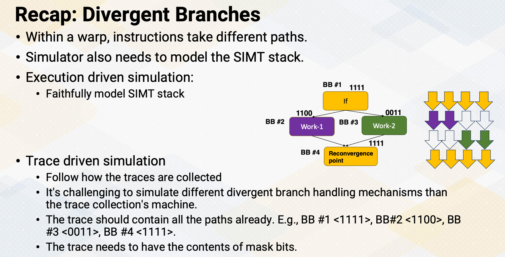
Let’s recap divergent branches. Divergent branch is called when within a warp instruction takes different paths. We reviewed how microarchitecture is implemented using the SIMT stack. The architecture simulator also needs to model the SIMT stack. In case of execution driven simulation, it can be done by faithfully model SIMT stack. Different ways of handling SIMT stacks can be modeled in the execution driven simulation. In the trace driven simulation, it has to follow how the traces are collected. Hence, it’s challenging to simulate different divergent branch handling mechanisms than the trace collection machines. To model divergence, the trace should contain all the paths such as BB #1 has 1111, but BB #2 has 1100, and BB #3 has 0011. And then branches are merged, so BB #4 has 1111. The trace needs to have these contents of the mask bits.
Memory Coalescing Modeling
Modeling memory coalescing is crucial. Memory requests need to be merged because it is critical to model the number of memory transactions and also bandwidth requirements. All memory source modeling is dependent on the number of memory transactions. Typically, this follows cache line sizes because memory requests are first accessed the cache and then it is already aggregated from the cache line granulity.
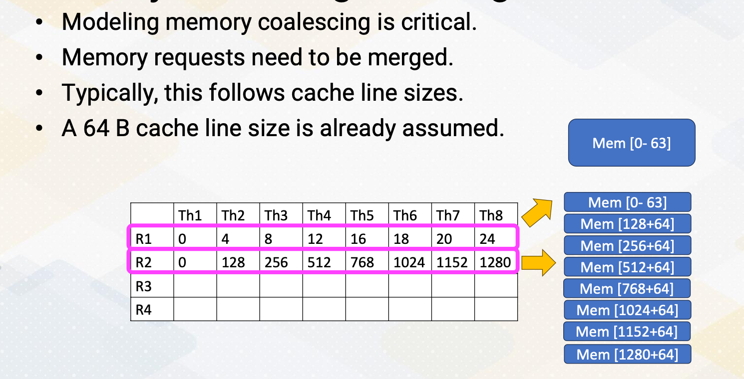
Let’s look at an example. A 64 byte cache line size is already assumed in this example. In the first memory request based on R1 register content, all memory access are coalesced and they generate only one memory request. In the second memory request, based on R2 register content, all memory requests are uncoalesced. Each individual memory request also generates 64 byte memory request.
Modeling Memory Coalescing with Trace
If you want to model memory coalescing traces, the trace should contain all the memory addresses from each work. The trace generator can insert all memory instructions individually, such as for va 1, 2, 3, 4 or trace generator already coalesces memory request, and this can reduce the trace size. In the previous example, the trace could contain separate memory requests such as address 0x0, 0x4, 0x8, 0x12, 0x16 etc., or it could just have 0x0 and the size information. The downside of this method is memory transaction size can be varied by microarchitecture. So this requires generate new traces if modeling microarchitecture use different memory transaction sizes.
Cache Hierarchy Modeling
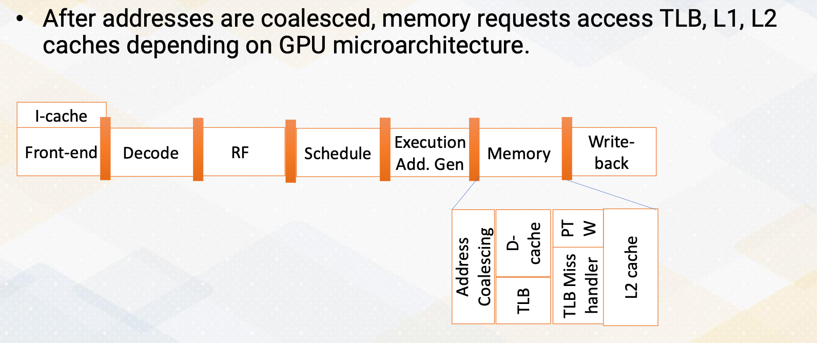
After memory addresses are coalesced, memory requests can access TLB, L1, L2 caches depending on GPU microarchitecture. The simulator can be also modeled by having different cache hierarchies. This is fairly similar to CPU modeling, but in the GPU modeling, memory coalescing is very critical.
Sectored Cache Modeling
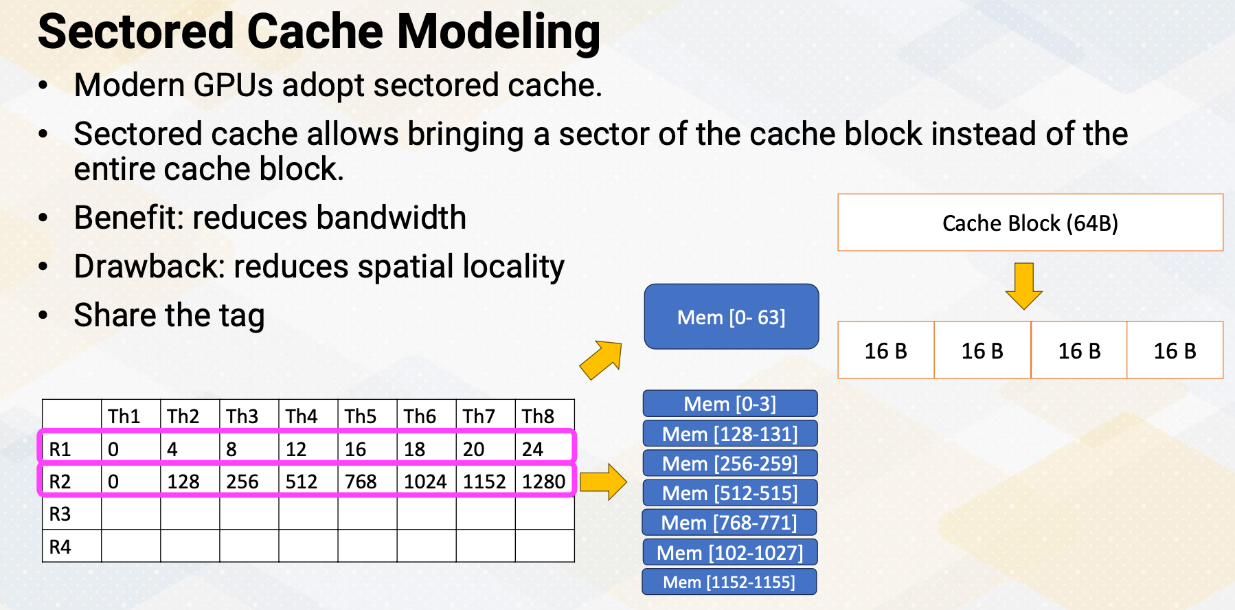
Modern GPUs adopt sectored cache. Sectored cache allows bringing a sector of the cache block instead of the entire cache block. The main benefit is it reduces the memory bandwidth. The main downside is it reduced spatial locality. In the previous example, the first instruction generates 64 byte request. So then we bring entire cache block. In the second instruction it generates 64 bytes of a memory request. But with a sectored cache, it can bring only one sector instead of the entire cache line, similar to here, only one 16 byte. And for the next memory request, again another 16 byte, for the next memory request, again, another 16 byte.
GPU Simulators
GPU simulators. Several open source GPU simulators are available. GPGPU-Sim which is the most popular simulator for modeling GPU models, NVIDIA PTX/SASS and it is an execution driven simulators. It is mainly targeting GPGPU. Accel-Sim which was developed by the same group as GPGPU-Sim is targeting for NVIDIA PTX/SASS and this is a trace driven and it is targeting more accelerators, MGPU-Sim models AMD GPU, and it is an execution driven. And the key feature is multi GPUs are supported. Macsim models NVIDIA and Intel GPU, and it is trace driven and execute heterogeneous computing. Gem5-GPGPU-Sim is combining Gem5, the most popular UCP simulator and the GPGPU-Sim. There are multiple versions. It could support AMD GPU or it could support NVIDIA GPU. It is also execution driven, and heterogeneous computing is modeled by executing both CPUs and GPUs. In this video, We reviewed CPU and GPU cycle-level simulation techniques. To support divergent warps, it is necessary to either model the SIMT stack or include mask bits inside the trace. Modeling memory coalescing is also one of the most critical part of the simulations.
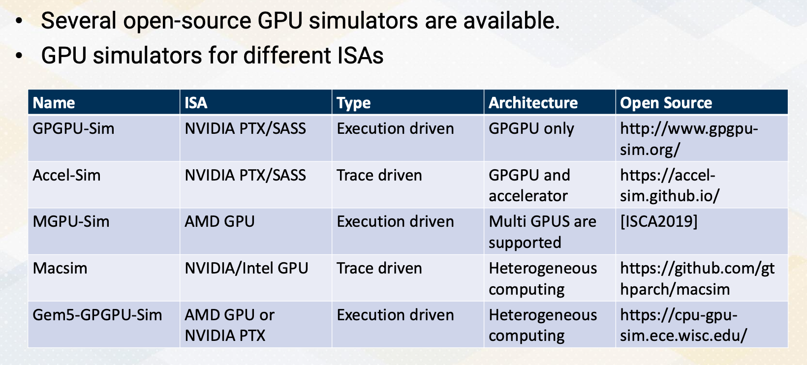
Module 8 Lesson 3 : Analytical Models of GPUs
Course Learning Objectives:
- *CPU and GPU cycle level simulation techniques are reviewed.
- Analytical model provides the first order of processor design parameters or application performance analysis.
- CPI computation was reviewed.
- Roofline was introduced.
- Compute bounded or memory bandwidth bounded is the most critical factor.
In this video, we will study analytical models of GPUs. Throughout this video, we’ll describe analytical models of GPUs. We’ll also apply analytical models to determine the first order of GPU design space explorations. And after this video, we should be able to explain CPI and interval-based analysis. The video will also describe the roofline model.
Analytical Models
Analytical models do not require the execution of the entire program. Analytical models are typically simple and capture the first order of performance modeling. Analytical models often provide insight to understand performance behavior. It’s simple, but it is much easier to understand. As an example of analytical model, let’s first try to design the GPU architecture.
First Order of GPU Architecture Design (1)
Let’s consider accelerating a vector dot product with a goal of 1T vector dot products per second. The target equation will be sum += x[i] * y[i]. For compute unit, we need to achieve 2T FLOPS operations, multiply and ADD, or 1T FMA/sec. FMA means floating point multiply and add, and many of FP operations are typically built for doing multiplication and accumulations. If GPU operates at 1 GHz, 1000 FMA units are needed. If it operates at 2GHz, 500 FMA units are needed. Memory units also need to supply two memory bytes for reading x and y array values, which means 2TB/sec memory bandwidth.
First Order of GPU Architecture Design (2)
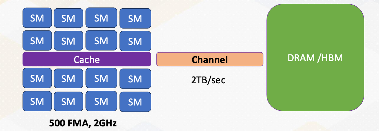
500 FMA units are approximately equal to 16 warps, if we assume the warp width is 32. If each SM can execute one warp per cycle at 2 GHz and there are 16 SMs, then it can compute 1T vector dot products. Alternatively, we could choose to have 8 SMs and each SM can execute two warps per cycle.
First Order of GPU Architecture Design (3)
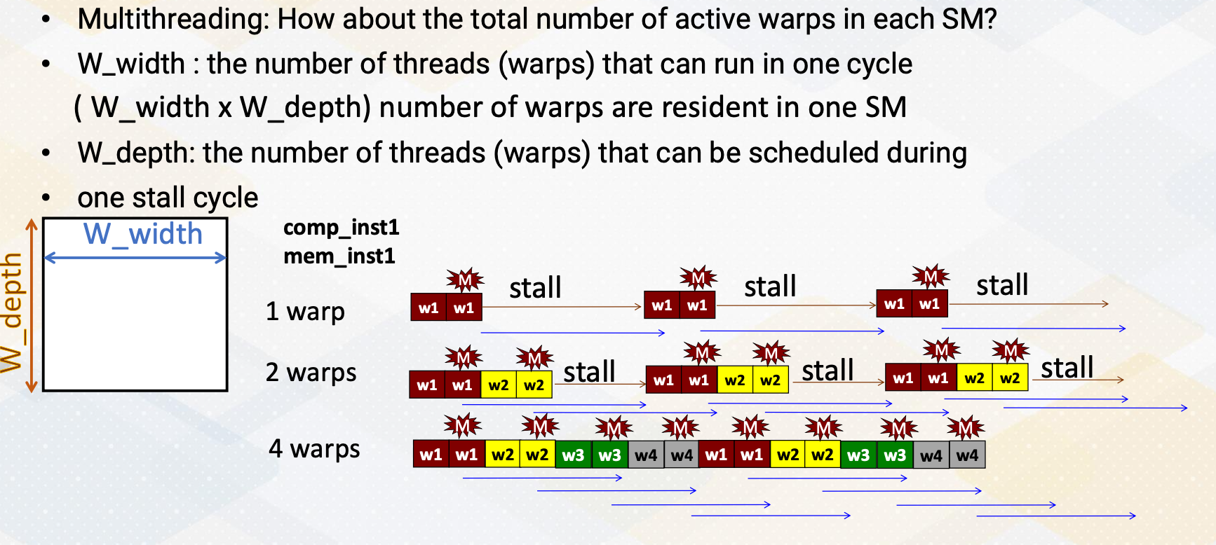
After we figure out the number of total FMA units, we also need to decide the multithreading design factors. In other words, we have to know the total number of active warps in each SM because in the previous slide it only computes the total execution time and bandwidth. To define the multithreading resource design factors, let me introduce the design parameters W_width and W_depth. W_width is number of threads that can run in one cycle such as 32. W_depth is the maximum numberof unique threads that can schedule during one stall cycle. So total W_width times W_depth number of threads can be executed in one SM. In this example, if you assume comp_inst and mem_inst for each warp. If there is one warp and if there is a memory instruction that generates a stall, then the pipeline has to be stalled until the memory cost is satisfied. If there are two warps, one additional warp can be scheduled during the stall cycle. If there are four warps, three additional warps can be scheduled, which can actually hide the stall cycles completely. W_depth indicates 1, 2, 4 in this example.
W_depth and W_width H/W Constraints
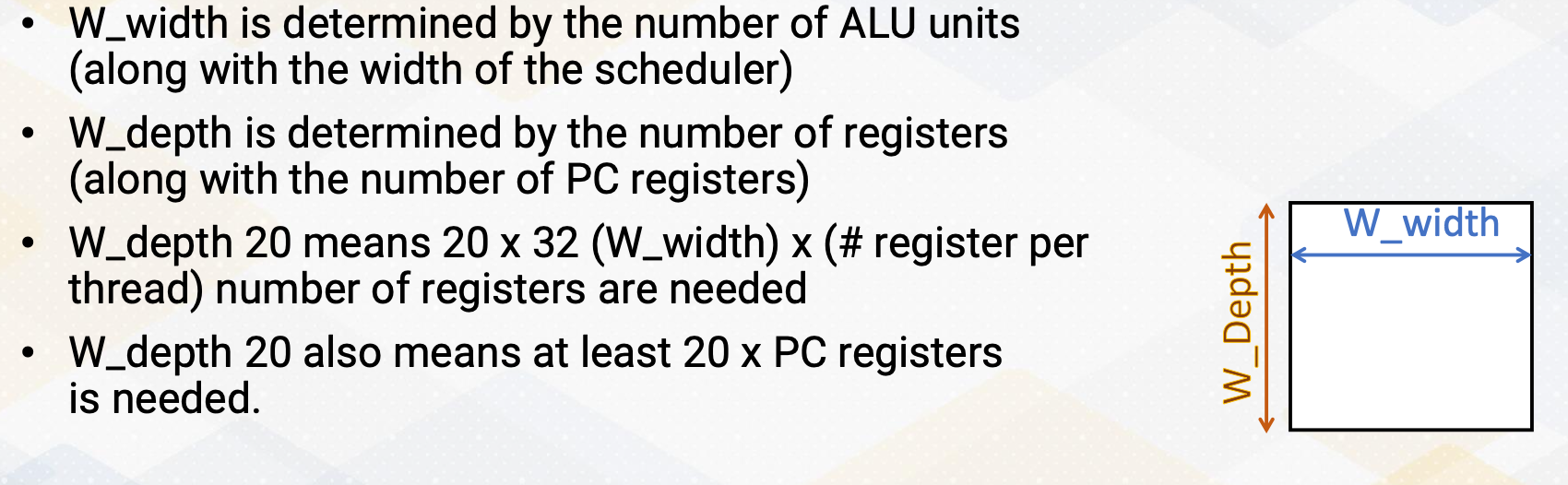
Then what decides W_depth and W_width in the hardware? W_width is determined by the number of ALU units, along with the width of the scheduler. W_depth is determined by the number of registers, along with the number of PC registers. W_depth 20 means 20 X 32, which is W_width assumption, times number of register per thread. In total, 20 X 32 times number register per thread, number of registers are needed. W_depth 20 also means that at least 20 X W_depth number of PC registers is needed.
Finding W_depth
How to decide W_depth? The design choice of W_depth is strongly correlated with the memory latency. If we use the dot product example and if we assume the memory latency 200 cycle, in the first case, there is 1 comp instruction and 1 memory instruction. Then to hide 200 cycles, 200/ (1 comp + 1 memory) which means 100 warps is needed. If you assume a different application, if you have 1 memory instruction per 4 compute instructions, to hide 200 cycles, 200/(1+4), which means 40 warps are needed.
Decision Factors for the Number of SMs
How do we also decide the number of SMs? Let’s revisit the previous example, which has 500 FMA units. We could have 1 warp X 16 SMs or we could have 2 warps X 8 SMs. Both give the same total number of execution bandwidth. The first option means large but fewer number of SMs, and the second option means small but many SMs. When we consider number of SM design decisions, we also need to consider the cache and registers need to be split across SMs. In other words, in the first case, it will be large cache for fewer SMs, in the second case, it will be small cache but for many SMs. Again, both also give the same size of total cache capacity. Large cache increases cache access time, but having a large cache, which are shared by multiple thread blocks, might increase cache hits when they are data sharing among multiple CUDA blocks. So this is a trade-off and we need to be a little more detailed analytical model to consider this effect. Sub-core can be also used as a design decision factor. And many of these decisions require more detailed analysis, especially the trade-off analysis between the size and access time.
Sub-core
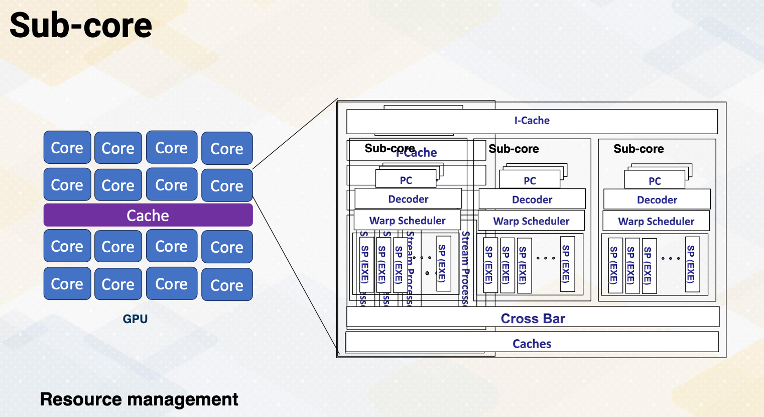
Sub-core. This is mainly for the resource management. So far, we have assumed that one core has a PC and one scheduler and execution units. In the sub-core, there are multiple sub-cores which have a similar structure as previous diagram, PC, decoder, warp scheduler, but these multiple sub-cores inside one SM share the same I-cache and large caches.
Roofline Model
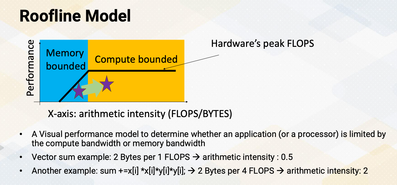
Let’s look at a roofline model. Here’s a diagram for the roofline. The Y-axis shows performance and since the performance chart looks like a roof, the name comes from that. This is a great visual performance model to determine whether an application, or sometimes a processor is limited by the compute bandwidth or memory bandwidth. Here the X-axis means arithmetic intensity, which shows how much floating point operations per byte. Then first in the right side, the yellow bound shows the compute bounded and the blue side shows memory bounded. The fuller side shows hardware’s peak flops, the compute peak performance.
Let’s look at an example. In the vector sum example, we need two bytes for one flops, which means arithmetic intensity is 0.5. This belongs to the memory bounded regions. But if you change an example to compute sum+=x[i]x[i]y[i]*y[i] in that case, we bring 2 bytes, the same as the vector sum x[i] and y[i], but we have to compute the 4 floating point operations. Then it increase arithmetic intensity to two. That moves this performance to this more in the compute bounded side. We can analyze the performance applications, whether these are memory bounded or compute bounded and whether there is room to improve performance by optimizing an application.
CPI (Cycle per Instruction) Computation
Let’s look at another example of performance modeling. The CPI, cycle per Instruction computation. The average CPI can be computed by CPI steady state plus CPA event1, event2, event3, etc. CPI steady state represent sustainable performance without any missed events. Then whenever there is a event, we can have CPI events.
Let’s look at an example of five stage in-order processor.
The CPI steady state equals 1. And CPI for branch misprediction event is three. And CPI for cache missed event is five. If an application has 2% instruction that has branch misprediction and 5% instruction that has cache misses then we can compute average CPI by computing 1+ 0.02*3, the frequency of event times the CPI of event. We can summate all this event. We also add 0.05 times five, which gives the average CPI. It’s very easy to compute average performance. In this modeling all penalties are assumed to be serialized.
CPI Computation for Multi-threading
Then can you expand this CPI for multi threading? Ideally CPI for multi threading equals CPI single thread/W_depth. W_depth is the number of warps that can be scheduled during the stall cycles which we have used in this video. By considering this effect, CPI multi-threading can be CPI ideal multi threading plus any additional resource contentions. The resource contentions could be MSHR which is related to the number of memory misses and busy state of execution units, and DRAM bandwidth, etc. Since GPU is an extension of multi-threading, we can utilize CPI modeling to model the GPU performance.
Interval Based Modeling: Extension of CPI Modeling
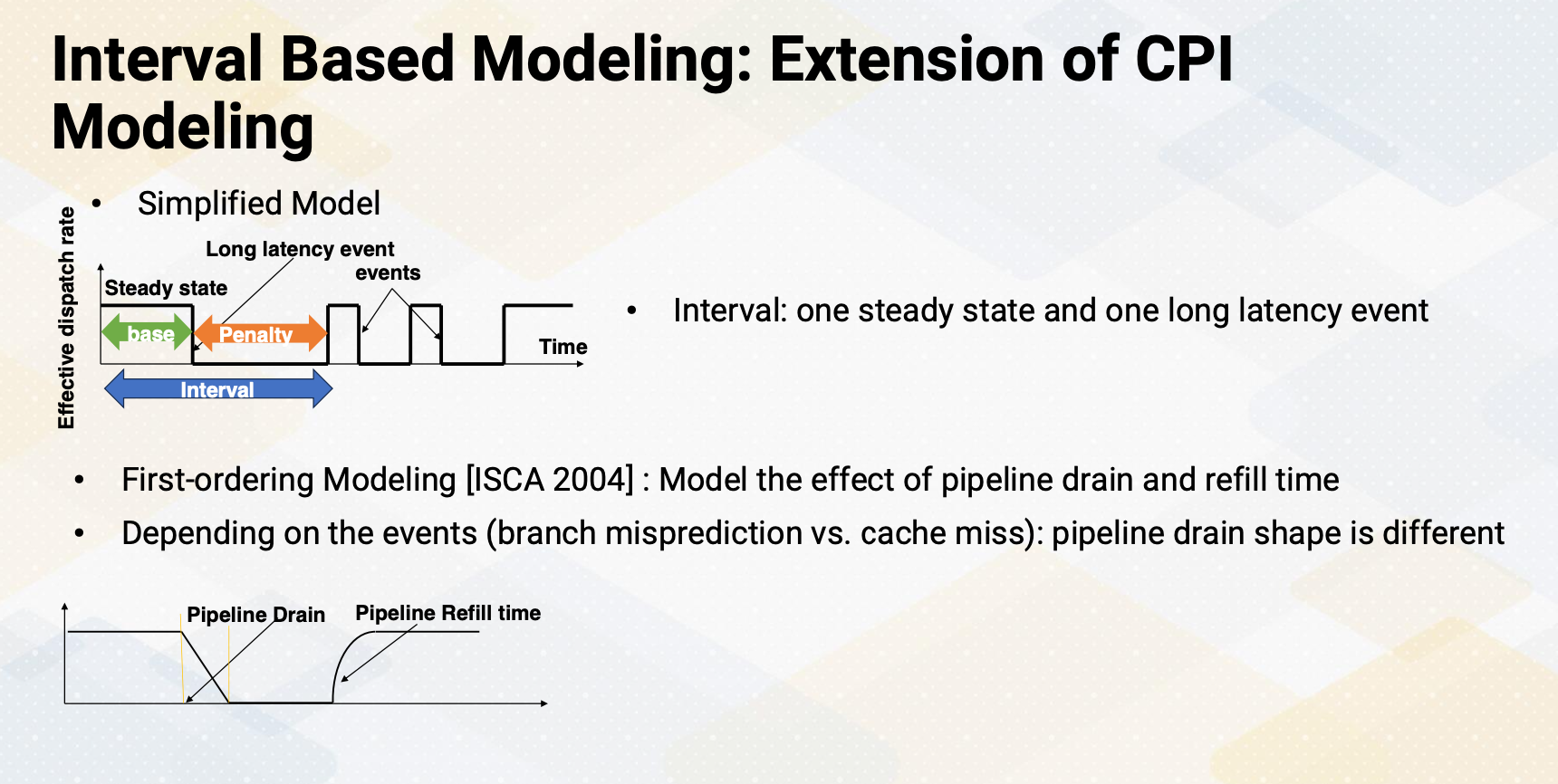
An extension of CPI modeling is an interval based modeling. In the simplified Interval based modeling, first an interval is defined in such that one steady state and one long latency event. So there is a steady state which has the same performance as effective dispatch rate. And then there is a penalty period. During the penalty period, none of the instructions are executed. And the ratio between the base and penalty is dependent on event. To improve this model first-ordering modeling was proposed in ISCA 2004 which modeled the effect of pipeline drain and refill time. Instead of the pipeline being stalled abruptly it models the slow down of the execution, similar to drain the pipeline. And when the pipeline starts to execute, it slowly refills. You can also look at the diagram such as that y-axis is a number of instruction that can be executed. And this method is called interval based modeling.
Applying Interval Analysis on GPUs
To develop an interval analysis for the GPU, the Naïve approach is to treat GPU as just a multi-threading processor. The major performance differences between GPU and multi threading processor would be caused by the following two important factors. First, branch divergence, because not all warps are active and some part of the branch code is serialized. Second, memory divergence, because memory latency can be significantly different depending on memory is coalesced or uncoalesced. To accurately model the GPU performance with interval analysis, these two factors need to be considered. And newer GPU interval analysis models improve the performance models by modeling sub-core, which we discussed briefly, and sectored cache and other resource contentions.
In summary, CPU and GPU cycle level simulation techniques are reviewed. Analytical model provides the first order of processor design parameters or application performance analysis. CPI computation was reviewed which has been used in many architecture studies. Roofline design was introduced. And compute bounded or memory bandwidth bounded is the most critical factor in deciding the performance aspect.
Module 8 Lesson 4 : Accelerating GPU Simulation
Course Learning Objectives:
- Describe techniques to accelerate simulation speed
- Identify challenges in cycle- level simulation
- Explore techniques for accelerating simulation
- Describe sampling based techniques
Hello, We’ll study techniques to accelerate GPU simulation. In this video, we’re going to talk about ways to speed up simulations. We will also discuss the challenges we face when simulating GPU architecture. We will also explore different methods for making GPU simulations run faster. Finally, we introduce techniques that involve sampling.
Challenges of Cycle Level Simulation
First, the problem with the cycle level simulation is that it takes a very long time. To give you an idea, if we simulate a speed of one kilo instructions per second, it would take us roughly 28 hours to simulate one billion instructions, which is just one second on a real machine. Imagine simulating machine learning workload that takes hours in a native execution. Simulation of this workload would take the time that is equivalent to a century of real world simulation time.
Accelerating Simulations
Now, let’s talk about how we can speed up our simulations. First, we can make the simulation itself run faster. Possible techniques are parallelizing the simulator to utilize parallel processors, event-driven simulation as opposed to a cycle level simulation. We can also simplify the model which might reduce accuracy, but often it increases the simulation speed significantly. Sampling techniques are commonly used. There is also statistical modeling and machine learning based modeling to build a simple model.
Second, reducing the workload itself,. We could use micro-benchmarks which represent the original program behavior. Or simply reduce the workload size such as use one iteration training phase instead of 1,000 iterations. If the workload is too complex, creating small representative workload is another approach.
Parallelizing Simulator
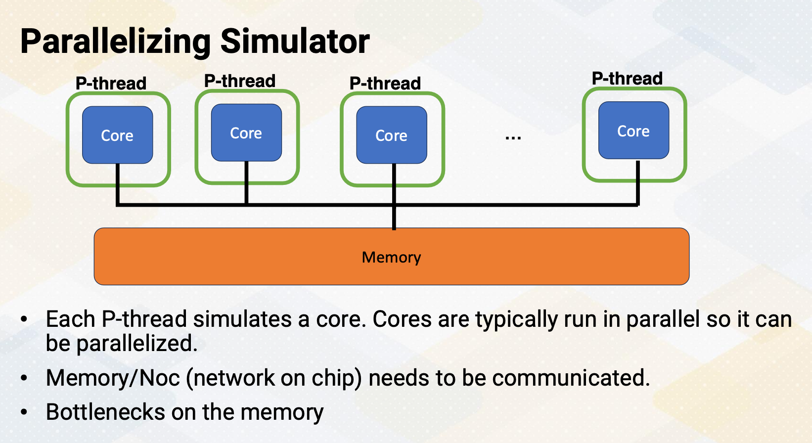
Parallelizing simulator. An easy way of parallelizing simulator is each thread models a core. However, there are some issues, especially with memory and communication between different parts of the cores. Although cores can be parallelized, such as communication, and memory would need to be serialized. Furthermore, these days most of the workfloads are memory bounded. So the modeling memory and communication would be performance bottlenecks.
Event Driven Simulation
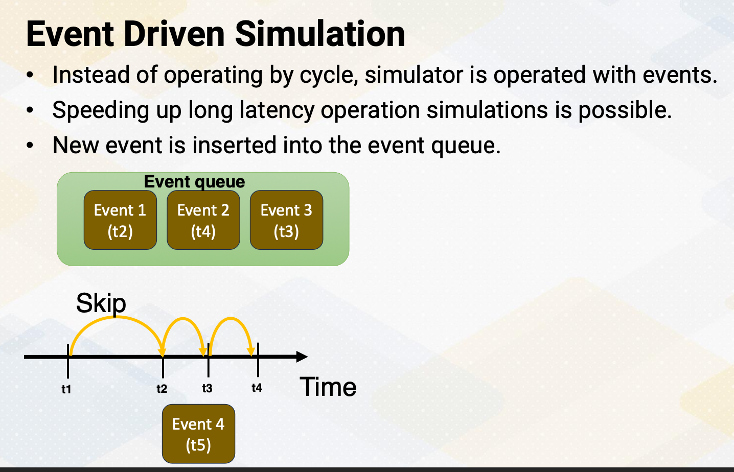
Event-driven simulation. Instead of going through each cycle, we can operate the simulator based on events. This can help us speed up simulations, especially when there are long delays involved, such as I/O operations. We write operations of NVM, which is known to be a long latency operation. With an event-driven simulation, the simulator just keeps adding new events to a queue and processes these events in order, and increments the time to the next event time.
Simplifying Models
Simplify models. Depending on what we’re simulating, we can simplify our models. We might use average values such as average latency or throughput for events that aren’t critical. Or the behavior is commonly consistent during the entire workload. It is important to know which events are critical to model or not. For example, when you model a pipeline processor, one option is to simplify the execution pipeline. Instead of modeling instruction/fetch/decode/execution, we could assume IPC is equal to issue width. Then model only caches and memory.
As a real example, z-sim CPU simulator simplifies the core pipeline. Another option is modeling a pipeline is to simplify the memory model as opposed to the first case. In this case, the simulator assumes memory system has a fixed latency. This is useful when it evaluates different computing models in a pipeline.
Sampling Techniques
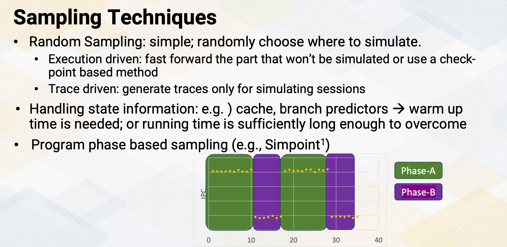
Sampling technique involves taking samples of the simulation. We can do random sampling where we randomly pick certain parts to simulate. There are also execution-driven sampling which let us skip parts that don’t need to simulate or use a checkpoint based method. Another method is trace-driven simulation where we generate traces for specific simulation sessions. When we use a sampling technique, we need to be careful how to handle state information. For example, for cache and branch predictors, warming up time is needed. Or by running a simulation for a long time, the initialization effect won’t affect the final simulation result. Instead of random sampling, detecting the program phase and simulating representative portion of the program is also very commonly used. Simpoint technique is commonly used for that purpose. As shown in the diagram, program has two phases, high IPC phase A which is represented as a green box area, and low IPC phase B which is represented as purple box area. And the program repeats these two phases. In this case, instead of simulating the entire application, we can simply simulate phase A and phase B only.
GPU Sampling Techniques
For GPUs, sampling techniques are slightly different. As GPU executes SPMD style program, one single thread’s execution length is too short. And instead, it has many number of threads. To address this, we can use block level sample, kernel level sampling, or warp level sampling. For example, in the CUDA block level sampling. We could simulate 100 CUDA blocks instead of thousands of CUDA blocks. Or for the kernel level sampling, we can simulate only one or two kernels instead of tens of kernels. These techniques can be very effective for machine learning workloads, since they repeat the same kernel for hundreds of times. Another approach is warp level sampling, which reduces the number of warps to simulate.
Reducing Workloads
Reducing workload techniques. As we discussed in the previous slide, we can reduce the number of iterations. Machine learning workload runs thousands iterations. Each iteration shows very similar characteristics. Hence, instead of 1,000 iterations, we can simulate only once. The second method is to reduce the input size. For example, a graph processing application traverses for one billion nodes. By reducing the input graph size, we could make the graph algorithm traverse only for one million nodes. In the third method, we just focus on the most important parts of a program or kernel to simulate. For example, a program has hundreds of functions, but only one or two functions dominate 90% of the application time. In that case, we can change the applications to run only those two kernels.
Data-Driven Modeling
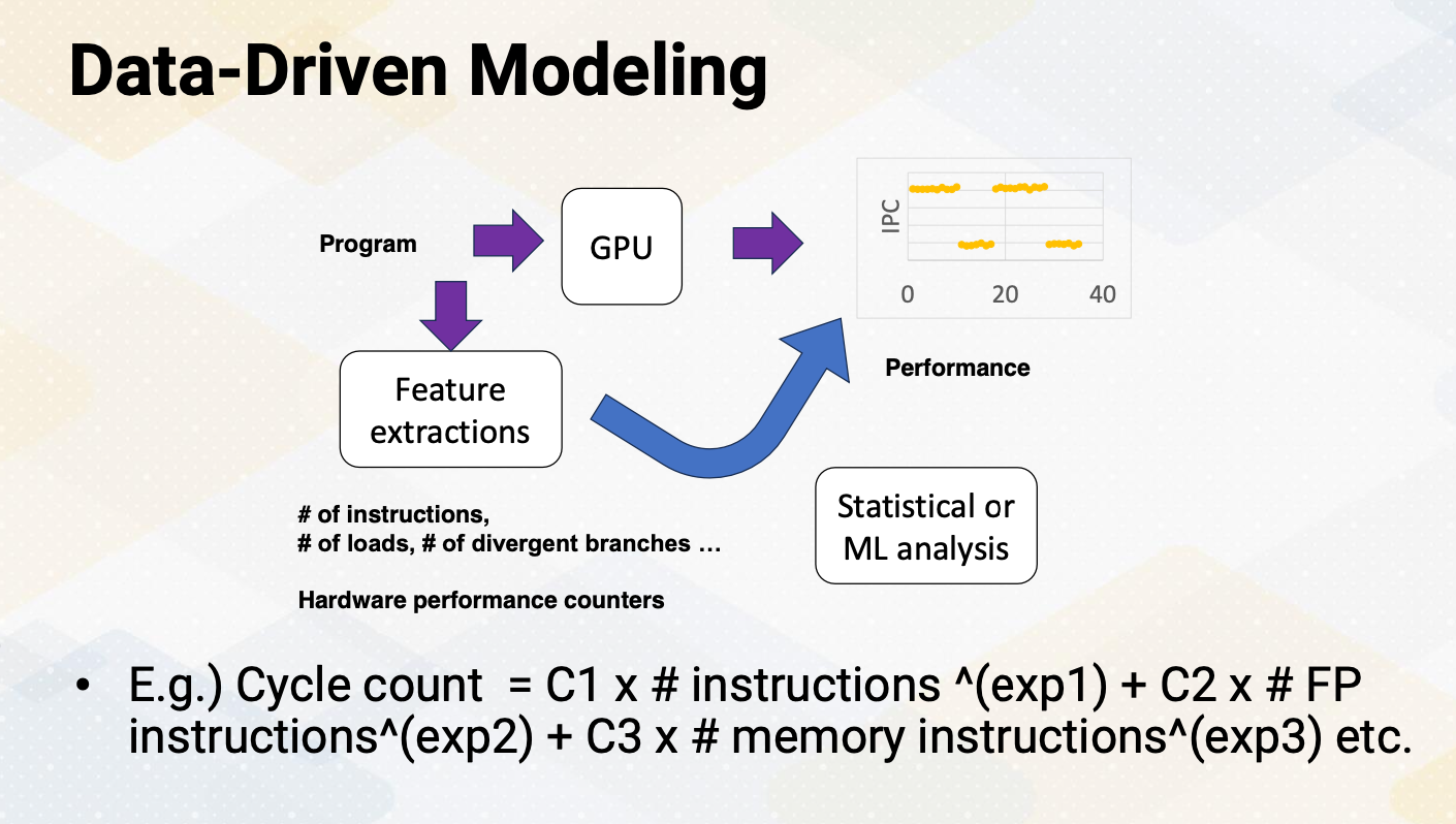
We might use data-driven modeling to figure out how to simplify the model instead of using cycle level simulator. This is somewhat similar to analytical model but instead of constructing the model based on the understanding the underlying architecture behavior, this approach is purely based on data to construct a model. First, by running an application on the hardware, it collects important statistics such as IPC. And then it collects other stats, such as the number of instructions, the number of loads, the number of divergent branches that can explain the program performance behavior. This step is similar to feature extractions. These events can be collected with hardware performance counters or using a simulator. And then use statistical or ML analysis to construct a model. A simple example can be following. The total cycle count is the sum of different event counter values times different coefficient values raise to a power. Such as cycle count is the sum of C1 times instruction count to the exponent 1 and C2 times floating point instruction count to the exponent 2, and C3 times memory instruction count to the exponent 3. The coefficients and exponent values can be found by collecting data and using a statistical or machine learning based modeling.
In summary, we talked about various techniques for making simulations run faster. We’ve placed a special emphasis on sampling and reducing the workload size.
Module 9: Multi GPU
Objectives
- Understand multi-GPU architecture
- Understand the challenges of multi-GPU architectures
- Understand how to increase concurrency on multi-GPUs
Readings
Required Readings:
- Arunkumar et al., “MCM-GPU: Multi-chip-module GPUs for continued performance scalability,” 2017 ACM/IEEE 44th Annual International Symposium on Computer Architecture (ISCA), Toronto, ON, Canada, 2017, (https://ieeexplore.ieee.org/document/8192482)
Optional Readings:
- https://www.nvidia.com/en-us/data-center/nvlink/
- https://developer.nvidia.com/blog/upgrading-multi-gpu-interconnectivity-with-the-third-generation-nvidia-nvswitch
- https://docs.nvidia.com/cuda/gpudirect-rdma/index.html
- Yu, Fuxun, Di Wang, Longfei Shangguan, Minjia Zhang, Chenchen Liu and Xiang Chen. “A Survey of Multi-Tenant Deep Learning Inference on GPU.” ArXivabs/2203.09040 (2022):
- Zhisheng Ye, Wei Gao, Qinghao Hu, Peng Sun, Xiaolin Wang, Yingwei Luo, Tianwei Zhang, and Yonggang Wen. 2024. Deep Learning Workload Scheduling in GPU Datacenters: A Survey. ACM Comput. Surv. 56, 6, Article 146 (June 2024), 38 pages. https://doi.org/10.1145/3638757
- https://docs.nvidia.com/deploy/pdf/CUDA_Multi_Process_Service_Overview.pdf
Module 9 Lesson 1 : Multi-GPU Hardware
Course Learning Objectives:
- Describe multi-GPU architecture
- Describe the challenges of multi-GPU systems
- Introduce thread block scheduling and memory management in multi-GPUs
- Explore alternative communication options in multi-GPUs
In this module we’ll cover multi-GPUs, which are commonly used for data center GPUs. In this video, we’ll discuss the hardware aspect of multi-GPU systems. The video will provide multi-GPU architecture and its core principles. The learning objectives of this video are, to understand the obstacles and complexities that multi-GPU systems present and how to address them. It will also provide an example of thread block scheduling and memory management techniques in the context of multi-GPUs. We’ll also explore alternative communication options designed specifically for multi-GPUs, offering enhanced data exchange capabilities.
Multi-GPUs
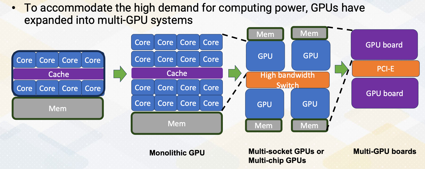
As the computing demand gets higher, GPUs have involved to scale up. First, GPU has evolved by increasing number of cores. However, in the monolithic GPU approach, the scaling would face several challenges, including cost, reliability. To overcome those challenges, the next way of scaling up is by connecting GPU chips using silicon interposer, or multi-sockets. After that, it even scale up by connecting the GPU board with multiple PCI Express connections.
Multi-GPU Connections
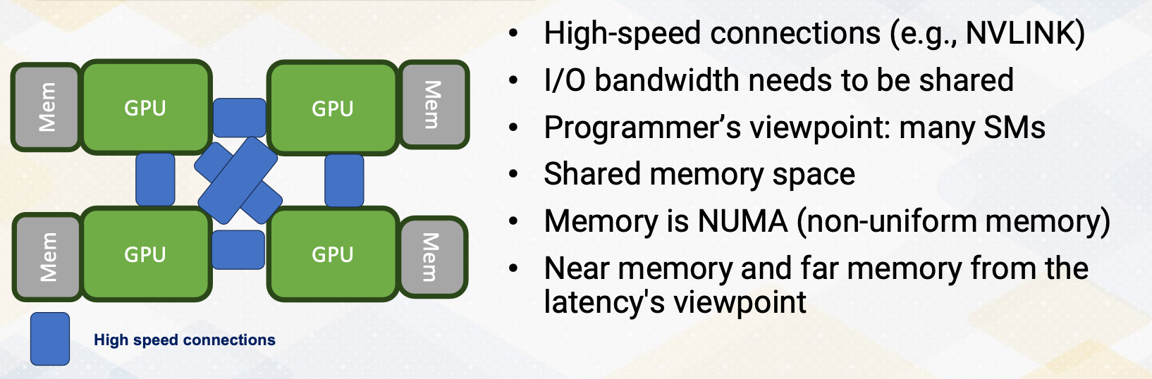
Let’s look at a little bit more on connecting multi-GPUs. To scale up packaging level integration of multi-GPU modules have shown up to build a larger logical GPUs, which can enable continuous performance scaling beyond Moore’s law. To accommodate the high bandwidth requirements of DRAM request, 3D stack memory like HBM has been connected. The entire systems, I/O bandwidth needs to be shared. In the NVIDIA, the connections is also done with NVLINK technology. Although the inside GPUs is composed of multiple GPUs, for programmer’s viewpoint, these are still just many SMs. All memories are accessible using global memory, which can be considered as a shared memory program space. The challenges is that memory is NUMA, non-uniform memory accesses which can be considered near memory and far memory in terms of memory latency and even for the bandwidth aspect, which brings two important questions.
How to schedule thread block in this GPU and how to allocate a page? One of the simple solution is to allocate the page in the near memory that the thread block is scheduled.
Thread Block Scheduling and Memory Mapping
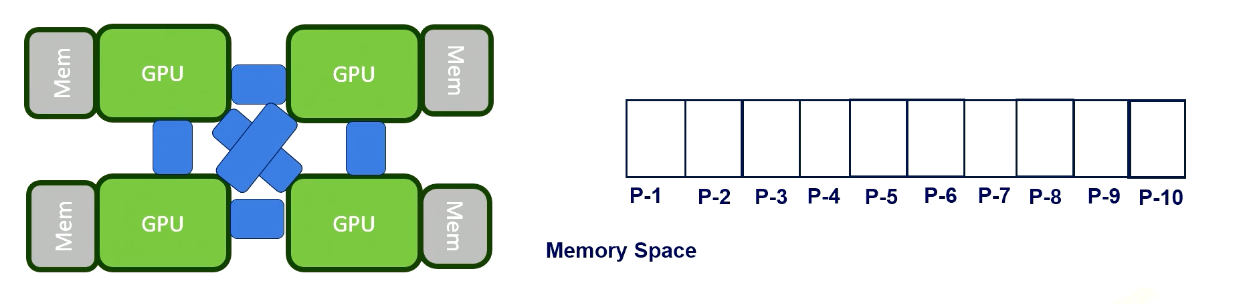
Here is an example. Let’s assume that there are several thread blocks and each of them use different memory areas.
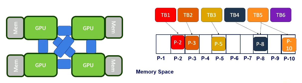
In a round-robing scheduling, each GPU will get different thread blocks. To make it simple, we just assume each GPU gets only one thread block. When the thread block request to access a certain page, the page will be allocated to the corresponding GPUs DRAM. This is first touch based allocations.
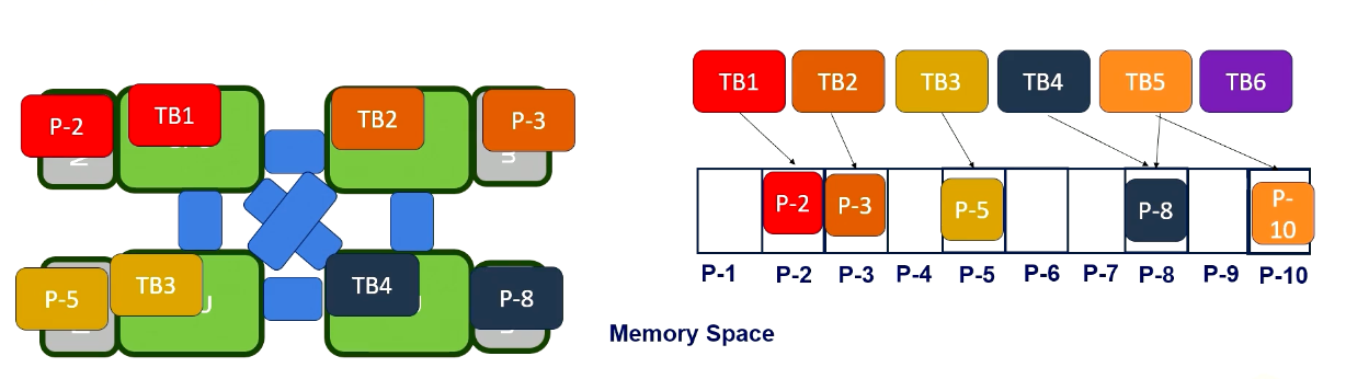
And after that, additional thread block will be scheduled. For example, Thread 5 is scheduled where thread block was originally scheduled.
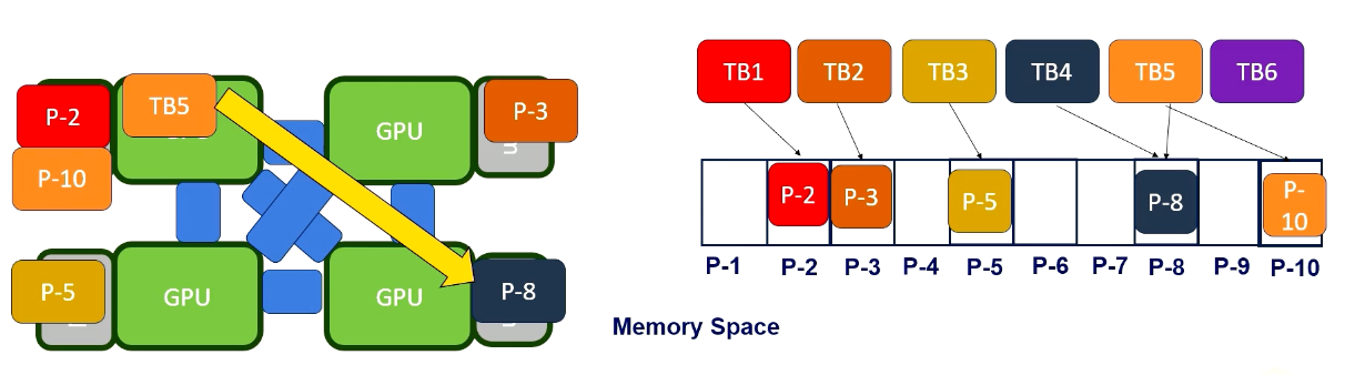
In this case, it will bring Page 10, but for Page 8, it becomes a far memory accesses. So it’s important to schedule a thread block on GPUs that utilize a memory locality.If the schedule allocates the thread block where Page 8 is located, Thread Block 5 would have only near memory accesses. As an alternative option, memory pages can be migrated if there are enough far memory accesses.
NVLink/NVSwitch
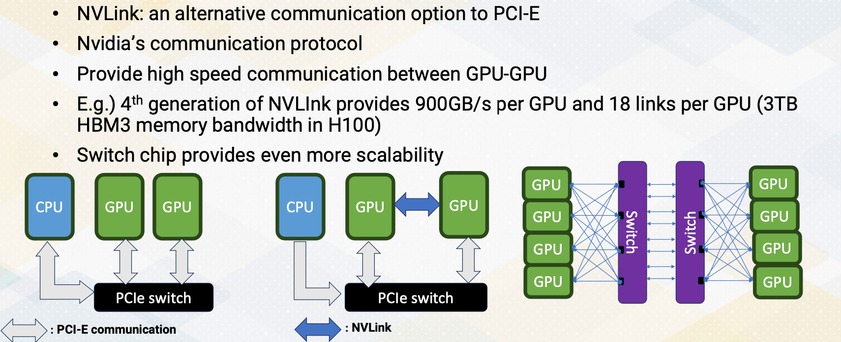
NVLink is an alternative communication option to PCI Express bus. It’s a NVIDIA’s communication protocol. It provides high speed communication between GPU to GPU. For example, fourth generation of NVLink provides 900 GB/s per GPU and it has 18 links per GPU. To give an idea, H100 has 3 TB/s memory bandwidth with HBM3. So NVLink has about one fourth of memory bandwidth. As the number of GPUs gets increased, to provide more scalability of point to point communications. NVIDIA introduced Switch which is called NVSwitch. Hence multi-GPUs are connected with the NVSwitch and NVLink, which provide higher bandwidth and shorter latency with many GPUs.
Memory Space
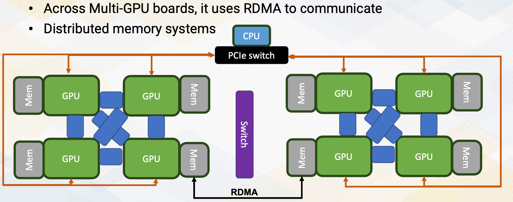
When memories are located through PCI Express bus, it will use different memory spaces. GPUs are connected with the PCI Express with the CPUs. But it doesn’t provide enough communication bandwith to communicate different GPUs memory spaces, hence across multi-GPUs board. It uses RDMA to communicate. This programming is more like distributed memory systems. The RDAM connections are point to point and all memories can be connected. But in this figure in the slide, to simplify this figure, we only show one RDAM connections.
Backgrounds: RDMA Technology
- Traditional communication
- Use TCP/IP like network to go through the network software stack
- Use CPU resource
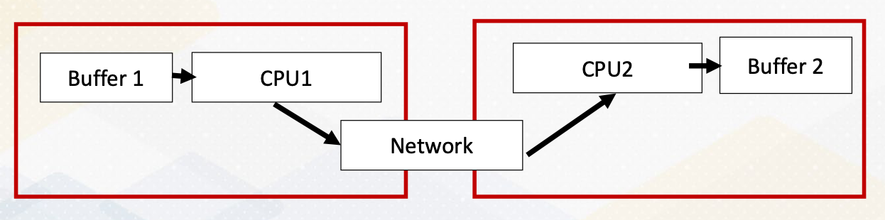
- RDMA: Remote Direct Memory Access
- Similar to DMA (Direct Memory Access), the communication between memory to memory can be done without using CPU resource.
- Host-bypass technology
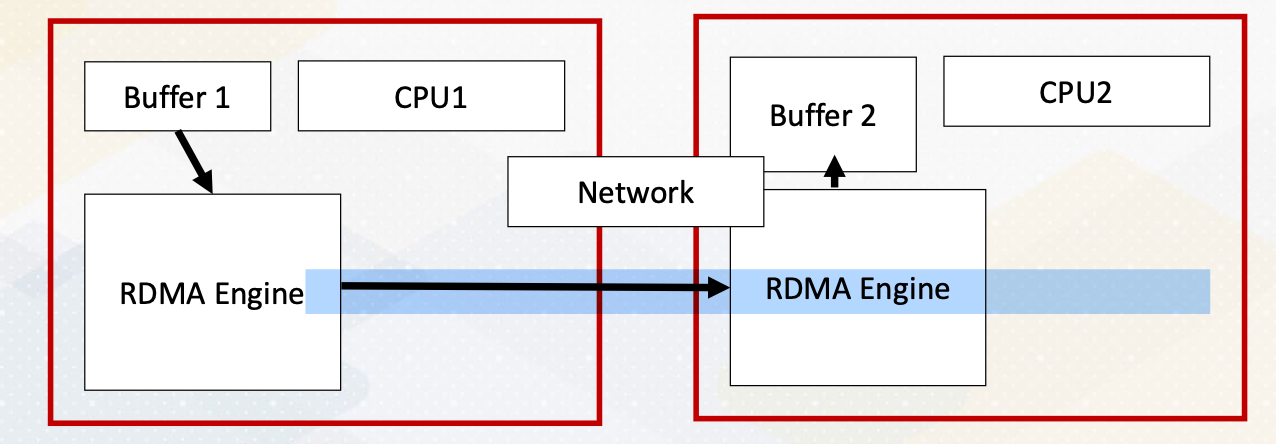
To provide a little bit background of RDMA. Traditional communication they use a TCP/IP like network, needs to go through the network of software stack and it uses the CPU resource to communicate. To send the contents of Buffer 1, it needs to go through CPU1 and CPU2 and then Buffer 2. This will use up CPU’s resource and also it can be also limited by CPUs busy status. RDMA stands for Remote Direct Memory Access. It is similar to DMA, Direct Memory Access, as it enables communication between memory to memory without using CPU resource. It is a host-bypass technology. With RDMA from Buffer 4, it can go to Buffer 2 directly without going through CPUs.
GPUdirect RDMA
In case of GPU, It also allows to communicate directly buffer to buffer by network interface, which it uses NVLink and NVSwitch. It can be also used to communicate between GPUs and even other third party devices. This RDMA and NVLink and NVSwitch work together. Since there are so many GPUs need to communicate each other, PCI Express bus cannot meet this high demand. In summary, in this video we introduced how to scale GPU. We explained different communication methods in multi-GPU environment. We also introduce NVLink and communication benefits. We also introduced RDMA technology and provided some background knowledge and also explained how GPUs can benefit from RDMA.
Module 9 Lesson 2 : Concurrency on GPUs
Learning Objectives
- Describe how to increase GPU utilization, particularly in the context of multi-GPUs
- Explore diverse strategies for efficiently managing multi-job workloads
- Discover different GPU concurrency mechanisms: Multi-Instance GPUs (MIG) and Multi Process Service (MPS), and Stream based programming
In this video, we will explore concurrency support on GPUs. Here, by the end of this video, we should be able to understand how to boost GPU usage, especially when dealing with multiple GPUs. We will explore various strategies to efficiently manage workload involving multiple jobs. We will discover different GPU concurrency methods including Multi-Instance GPUs, MIG, Multi-Process Service, MPS, and Stream based programming. Multi-GPUs offer impressive computing power.
Increasing Utilization of GPUs
GPUs are great for handling multiple data tasks. Well, not all jobs can utilize the provided GPU computing power, so how can we make better use of them? This is even more critical for GPUs in data centers. Traditional data centers deal with multiple tenant jobs, whereas some workloads like LLM, consumes all GPU resource with just single tenant. The usage patterns are totally different from traditional data center workload. Therefore, some AI workload performance is limited by the slowest task.
GPU Concurrency Mechanisms
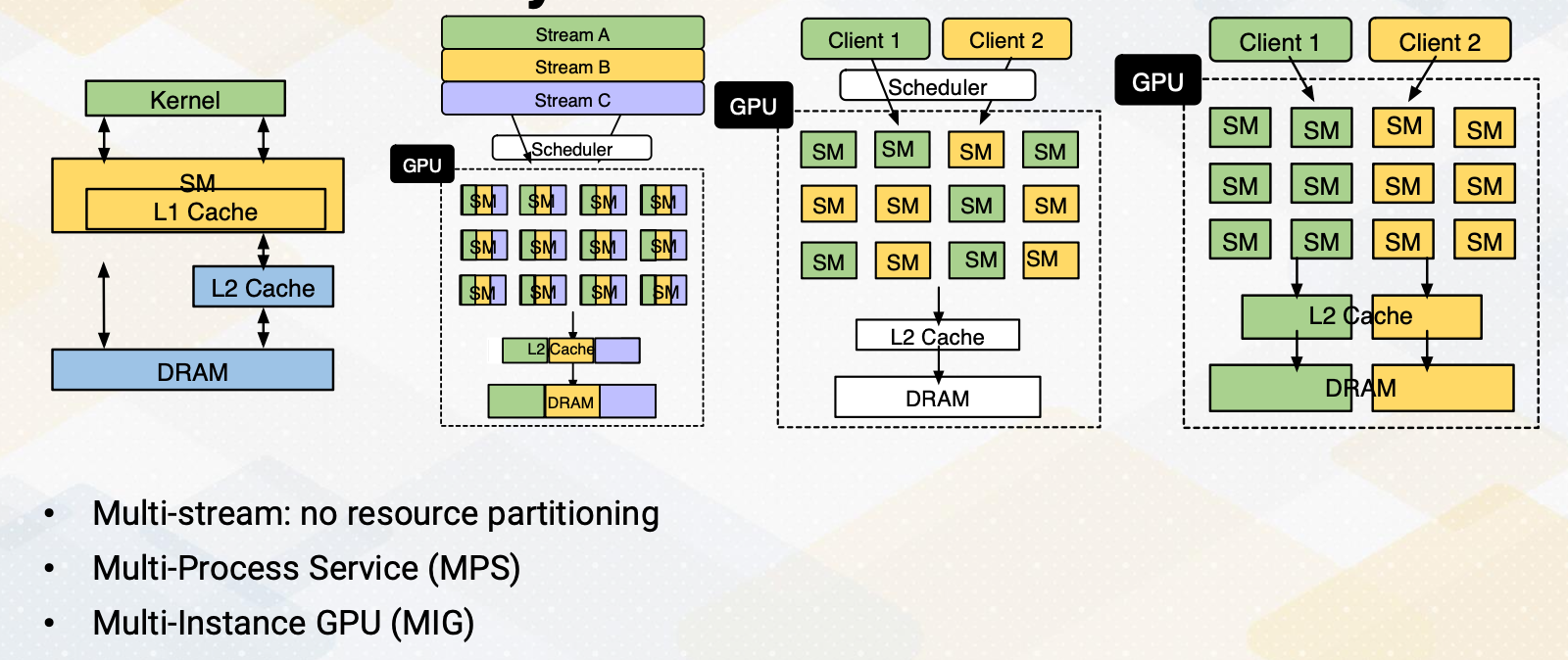
This slide illustrates different GPU concurrency support mechanisms. First we see the overview of GPU architecture. It shows SM which includes L1 cache and L2 cache. Then we have a DRAM. When you use stream feature in programming, multiple streams can be executed on GPUs. Only independent stream can be executed concurrently and stream is typically coming from one client. Multi-Process Service, MPS, where different clients are using different SMs, but the rest of the resource is shared. In Multi-Instance GPU, MIG, GPUs can be effectively separated for each client.
Multi-Instance of GPUs (MIG)
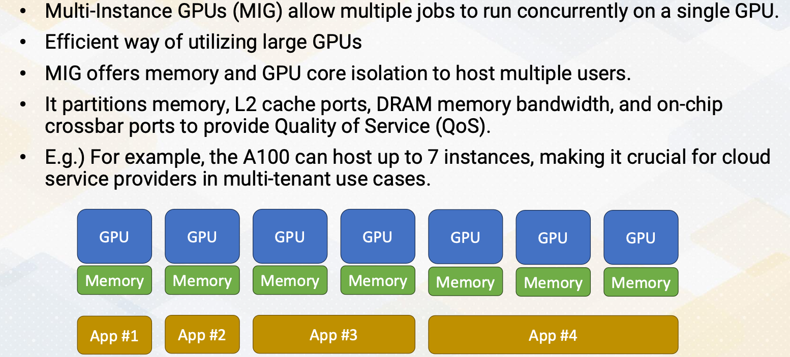
Multi-Instance GPU, MIG, allows several jobs to run simultaneously on a single GPU. This provides to be an efficient way to harness the power of the large GPUS. MIG provides isolation for memory and GPU cores, accommodating multiple users. It also divides memory, L2 cache ports, DRAM memory bandwidth, and on-chip crossbar ports, ensuring quality of service, QoS. For instance, the A100 can host up to 7 instances, making it vital for cloud service providers in multi-tenant scenarios.
Multi Process Service (MPS) Support
On the other hand, spatial partitioning of multi process service support is available starting from V100 GPU. Before that it was only supported with only time slicing. It enables multiple jobs to run concurrently, but doesn’t strictly partition resource, potentially leading to unpredictable performance. MPS methods can facilitate porting of MPI jobs to CUDA. In some cases, MPS may offer better utilization than MIG, especially when QoS isn’t a critical concern.
Example of Stream Based Programming
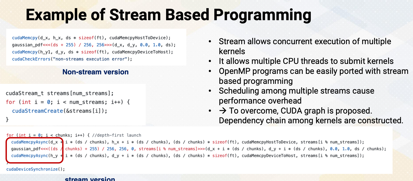
Stream allows concurrent execution of multiple kernels. It allows multiple CPU threads to submit kernels. It overlaps between communication and computation across different streams. In the stream version, you will see Cuda MemCpyASYCN. OpenMP programs can be easily ported with the stream based programming. Scheduling among multiple streams can cause performance overhead because dependency needs to be checked. To overcome this, CUDA graph is proposed to construct dependency chain before a kernel launch.
Example of Programming for Multi-GPU
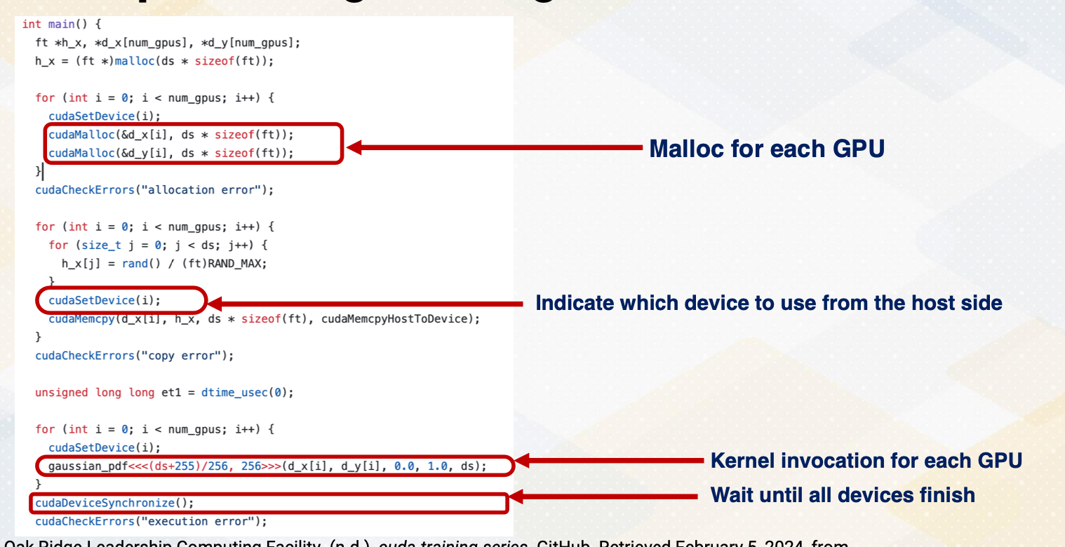
Now let’s look at another example of using multiple GPUs. First, it allocates memory for each GPU. So different GPUs have different memory object. We also call cudaSetDevice to indicate which device to use from the host side. Now we call gaussian_pdf for each GPU, separate kernels are invoked. After that, we wait until all devices finish. Please also note that multi streams can be also used with multiple GPUs.
GPU Support for Multi-Tenant Computing
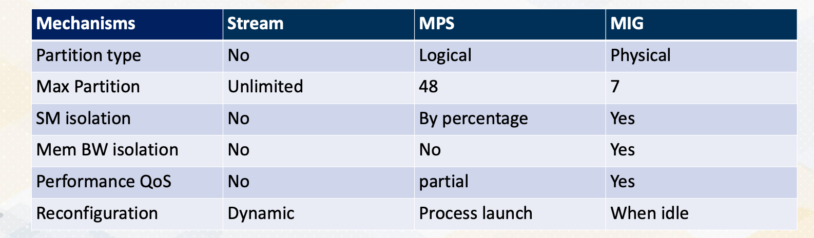
This table summarizes different techniques streaming MPS, MIG. It shows different partitioning types and how the SMs are isolated, how memory bandwidth is isolated. And also explains each technique provides performing QoS and when these partitioning can be performed. In summary, we have explored GPU concurrency methods, including multi instance GPU, MIG and multi process service, MPS. Additionally, we also introduced the concept of stream based programming for multi-GPU scenarios.
Module 10: Compiler Background - I
Objectives
- Be able to explain comparisons with other GPU programming
Readings
Required Readings:
- OpenCL overview
Module 10 Lesson 1 : GPU Compiler Flow
Learning Objectives
- Demonstrate comprehension of the fundamental process of GPU program compilation
- Explore the components and stages involved in GPU compilation
In this module, we’ll study backgrounds of compiler. In this video, first, let’s understand the fundamental process of GPU program compilation. We’ll also explore the components and stages involved in GPU compilation.
Compiler Flow
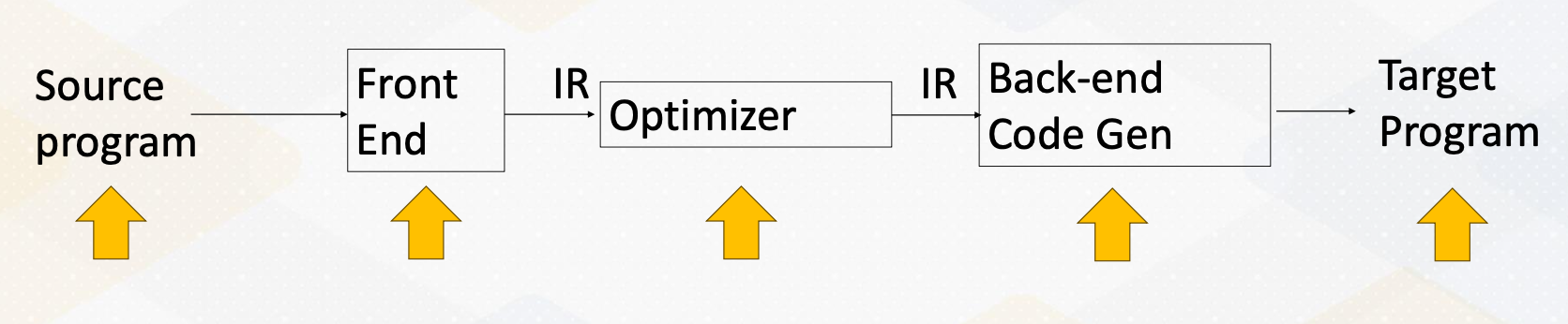
Here is a typical compilation process. There is a source code and the front end compiler converts the source code into IR. And the compiler optimizer performs several optimizations using IR. And then backend code generation performs machine specific target optimizations and then it also emits a target program.
GPU Compilation Flow
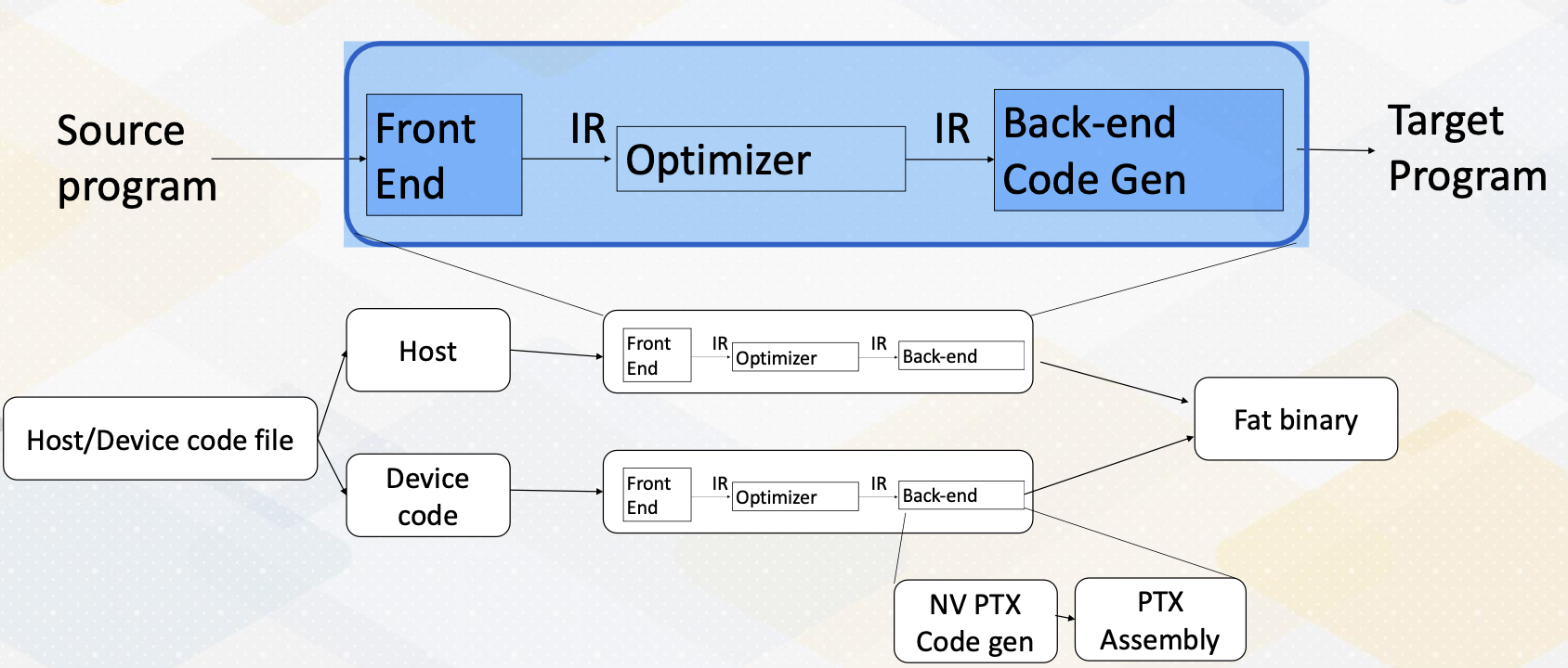
Here, the GPU compilation process. It follows similar process. One interesting part of GPU code is that it has host code and device code. The code gets split and then they will go through the same compilation process. For NVIDIA GPU’s case, it will eventually generate NV PTX code and then PTX assembly code will be combined with host and device code, then it becomes a fat binary.
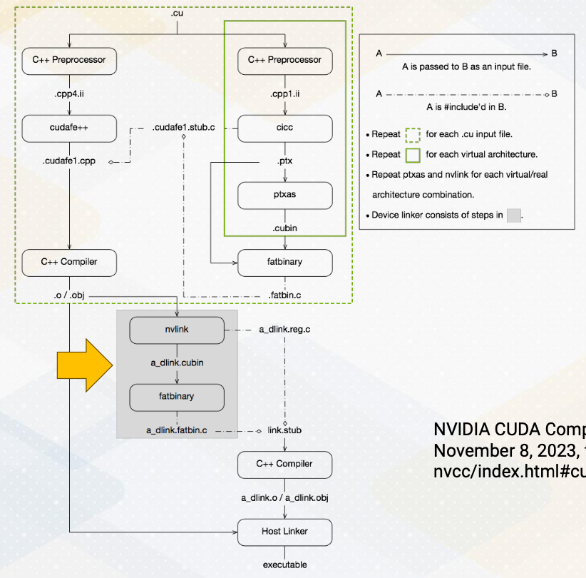
Here is a diagram from NVIDIA which shows more complex steps. This includes also linking steps. NVIDIA uses runtime library which runs on the host code and also it has many libraries, so linking steps are crucial. Since PTX is a virtual ISA, the architecture is also called virtual architecture. You will find the descriptions about virtual architecture in this diagram.
GPU Compiler Pass
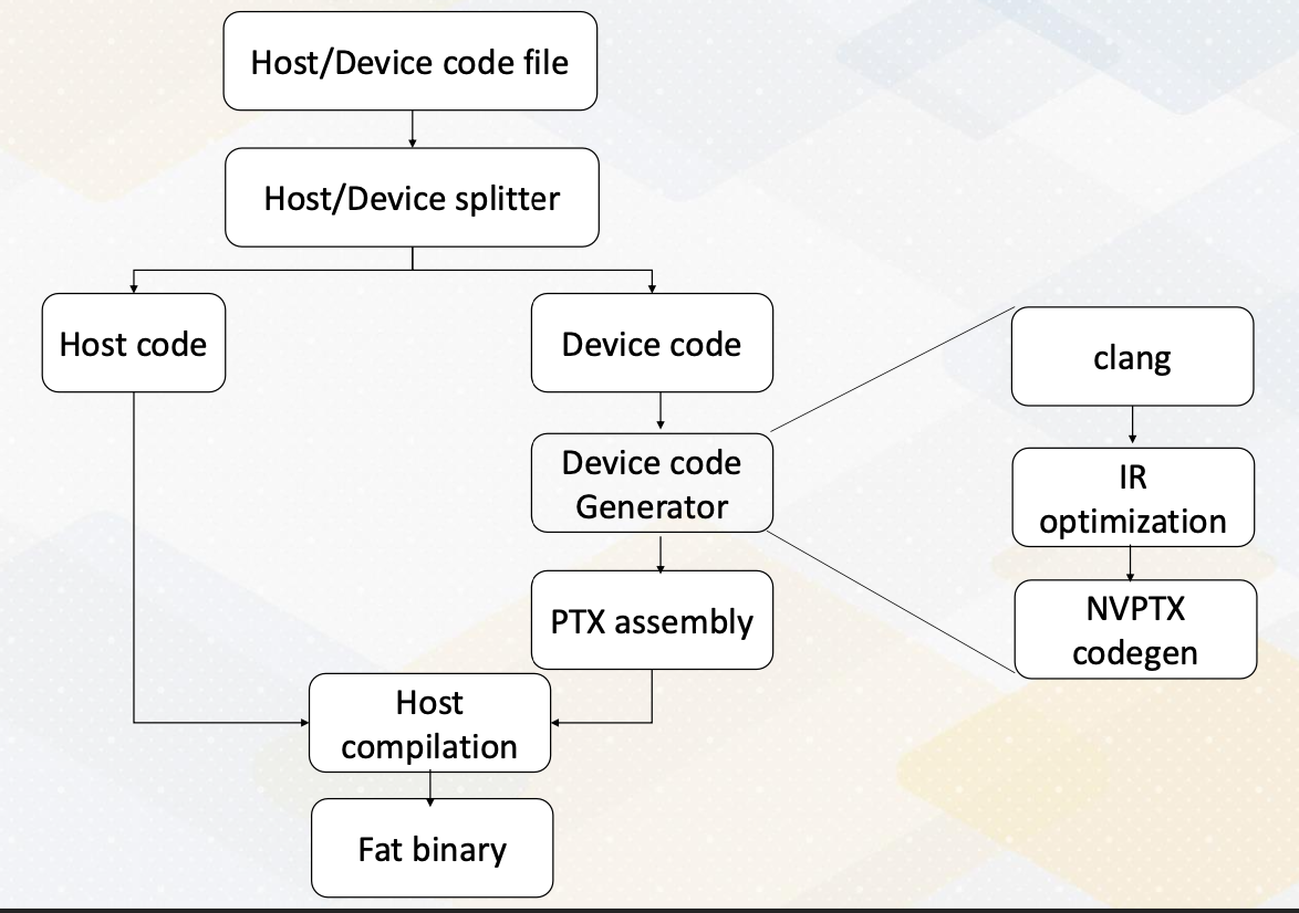
This slide shows the first open source version of full CUDA program compilation tool chain. It shares similar passes with NVIDIA GPU compilation process. In the device code generation, it has a clang, and IR optimization and then NVPTX code generation.
Roles of CLANG
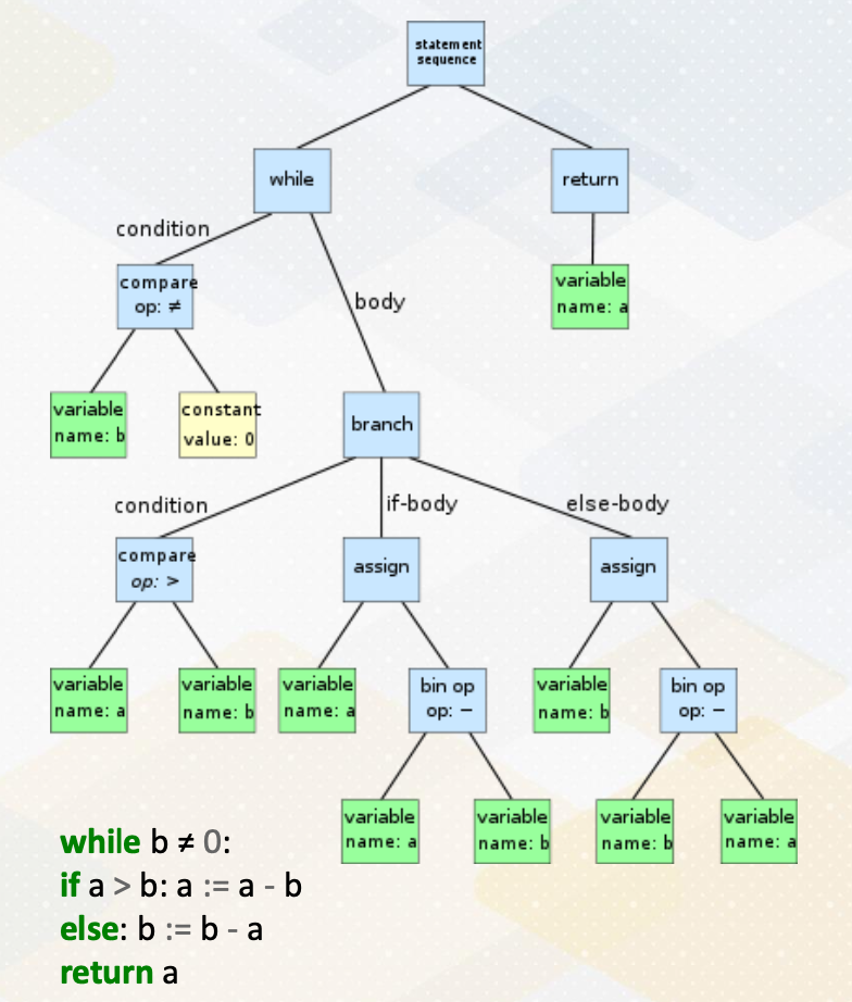
Just a couple of tool introduction. The roles of Clang are first, it is the front end parser. It is a tool chain for C-family languages, but lately it got extended to support other programming languages. It generates the abstract syntax tree AST. The right side of the slide shows an example of AST from Wikipedia. The figure is an AST from the bottom code which computes delta. This simple code can generate this much complex AST. The unit of definition in the node is depending on the usage of AST.
C++ PreProcessor
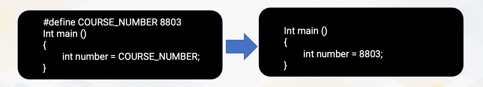
Next, C++ preprocessor. It performs text substitution for compilation. For example, in this slide it shows that there is a defined course Number 8803. After preprocessing, this course number is replaced with 8803. That’s to be done by this C++ preprocessor.
IR Optimizations
What are in the examples of IR optimizations? IR is an intermediate representation, which will be discussed in the next video in more detail. They are in the back-end compiler process. IR provides a good way to share the compiler infrastructure across different program languages and different architectures. IR provides a good abstract and to perform many compiler optimizations. And IR also contains many meta data to carry program information to help compiler process.
PTX vs. SASS
Let us discuss a little bit more about PTX and SASS. PTX is a parallel thread execution, and PTX is a virtual ISA, which means it is architecture independent. And a PTX will be translated into machine code later. Because this is architecture independent, it doesn’t have a target machine information, so PTX doesn’t have register allocation.
On the other hand, SASS is a real low level assembly language. It is an abbreviation of shader assembly. And this is architecture dependent assembly code, and it has target information so registers are allocated. If you have one version of a SASS code, and if we get a new GPU architecture, then the SASS code will be different in one or new version of GPU architecture, while in the PTX code will be the same across different GPU architectures.
Fat Binaries
In general, fat binaries contain execution files for multiple architectures. In the GPU’s case, it supports multiple GPU versions and also it has host code. GPU compilation provides one binary, but this fat binary will be split. again for host and device at run time. And the device component will be sent to a device driver. And it is common that device driver code will recompile this device code and send it to the machine. In this video we recap the terminology of PTX, SASS, Clang, IR and fat binary. We also reviewed the overall compilation process for GPU programs, including its key stages and components.
Module 10 Lesson 2 : PTX
Learning Objectives
- Explain the basics of PTX
- Explore PTX instruction format
- Describe optional predicate information
- Understand PTX code examples
In this video, we will discuss PTX. The learning objectives of this video are explaining the basics of PTX, and exploring PTX instruction format, and describing optional predicate information. And then we’ll be able to understand PTX code examples.
PTX Instruction
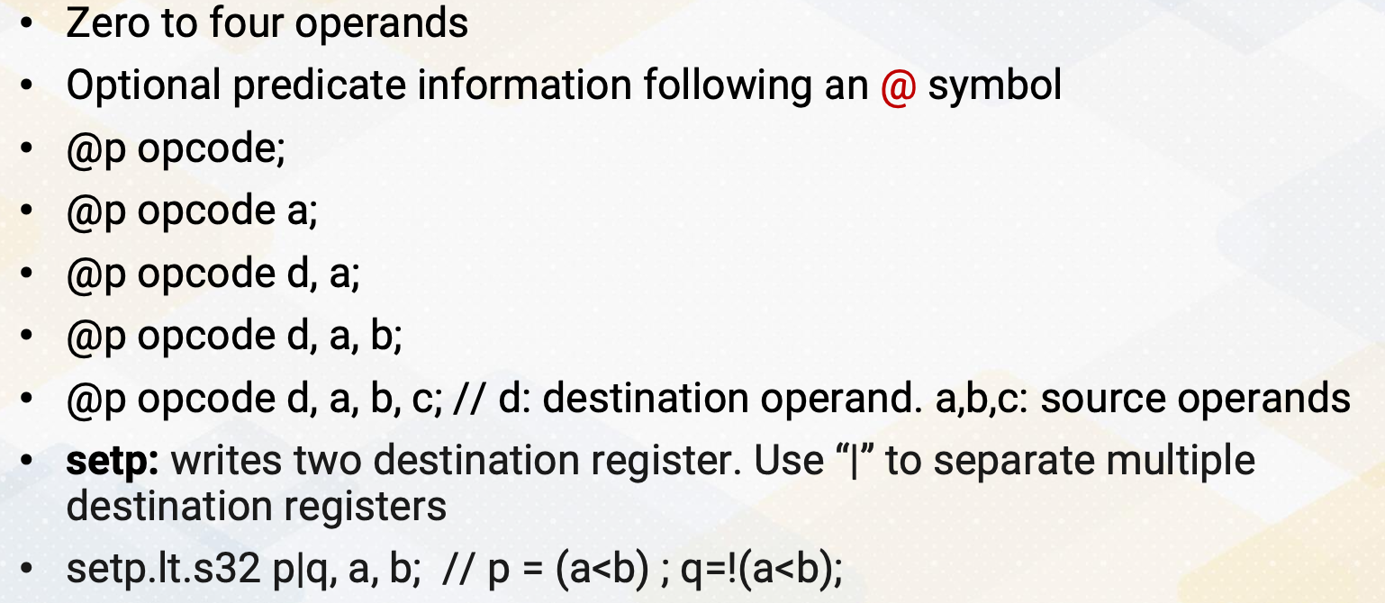
PTX instructions, here are the examples. PTX has zero to four operands. And it has optional predicate information following an @ symbol such as @p opcode, @p opcode a, etc. In @p opcode d, a, c, d is a destination operand and a, b, c are source operands. One of the important instructions in the PTX is setp, which writes two destination registers. It uses vertical bar to separate multiple destination registers. For example, setp.lt.s32 p vertical bar q, a, b. This instruction sets p = a less than b, and q is an opposite of p.
Predicated Execution
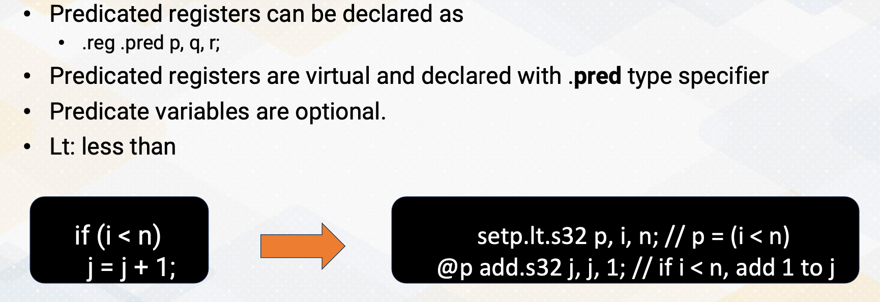
As we discussed earlier model, GPUs heavily use predicate execution to remove divergent branches. Predication is optional, so it follows @ symbol. And predicate registers can be declared as .reg, .pred, p, q, r. And .pred type specifier is needed, because all registers are virtual in PTX, so we need to specify predicate register information. The slide’s example shows if statement, and that is changed to predicate execution if i is less than n and j = j+1. This statement becomes two instructions. First setp instruction which is set up predicate value, and then the add instructions are predicated with p and add s32 j, j, 1. And here lt means less than.
Example of PTX Code
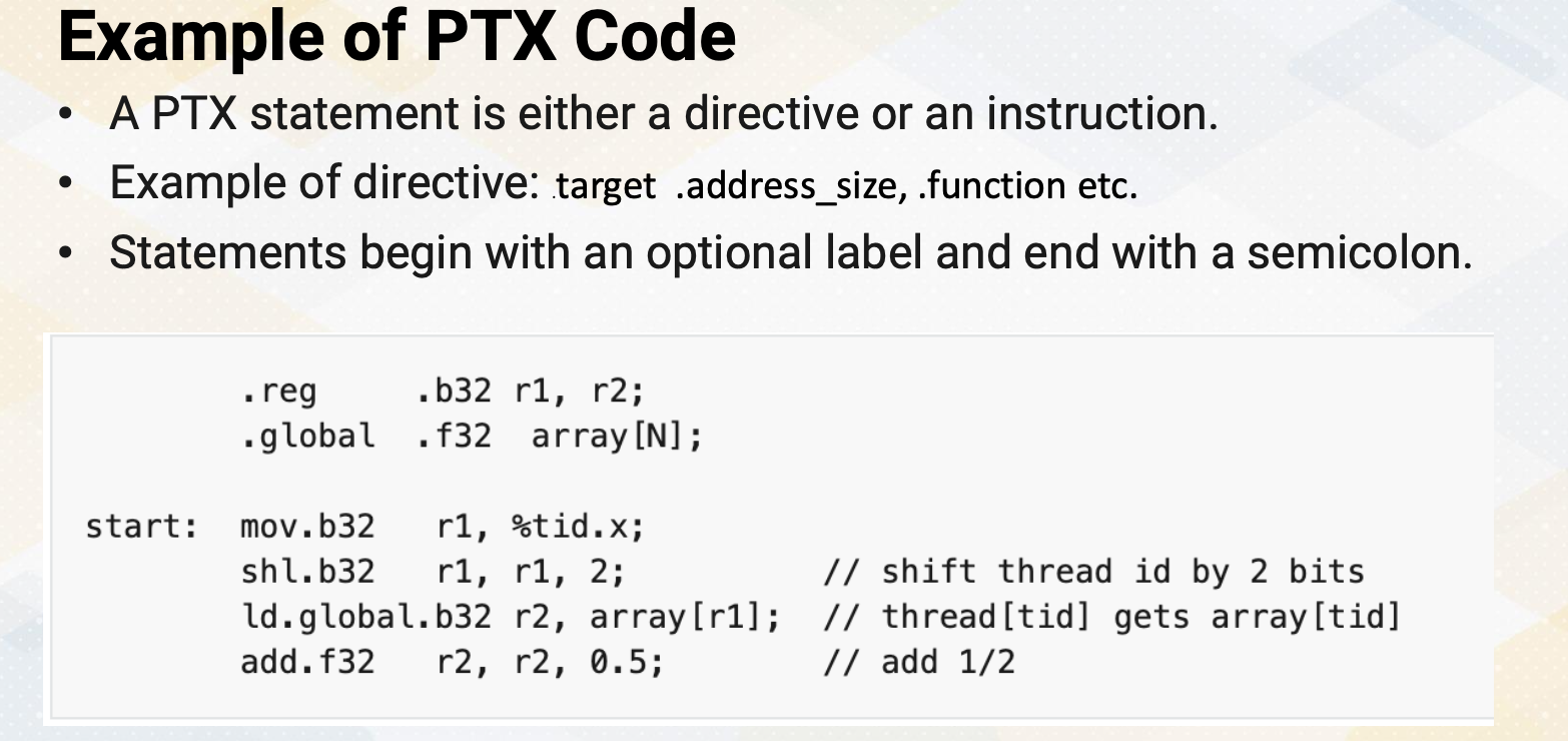
Here is more examples of PXT code. PXT statement is either a directive or an instruction. Example of directives are target, address_size, function etc. Statement begins with an optional label and end with a semicolon. Here in this slide, we see directives to set up registers and global memory variables, and label start indicates a starting of program. And we see move, shift, load and add instructions. And we’ll also see that all instructions have a type which indicates designation value types.
Other PTX Instruction examples
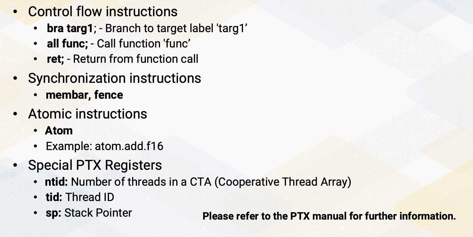
Here are other PXT instruction examples. Control flow instructions are bra targ1, which shows a branch instruction targeting label targ1. all func calls function name func, ret to indicate return from function call. There are also several synchronization instructions, membar, fence, those are for memory barrier and fence operations. Atomic instructions are indicated with atom prefix such as atom.add.f16. CUDA has many atomic operations including integers and floating point. So it is important to specify the type. There are also several special PXT registers. ntid is number of threads in a CTA, tid is thread ID, and sp is stack pointer. This is just a subset of PXT instructions, and you can find a complete set of PXT instruction in the PXT manual.
In this video, we reviewed PXT instructions. We also studied how PXT code is written for predicate execution to emphasize the importance of predicated execution. We also reviewed various examples of PTX instructions, including control flow, synchronization, and atomic instructions.
Module 10 Lesson 3 : IR and Basic Block
Learning Objectives
- Describe intermediate representation (IR)
- Identify basic blocks within code
- Construct a control flow graph
In this video, we study IR and basic block. Here are learning objectives. This video will describe intermediate representation, IR, and it will also teach how to identify basic blocks within code, and it will also show an example of constructing a control flow graph.
IR
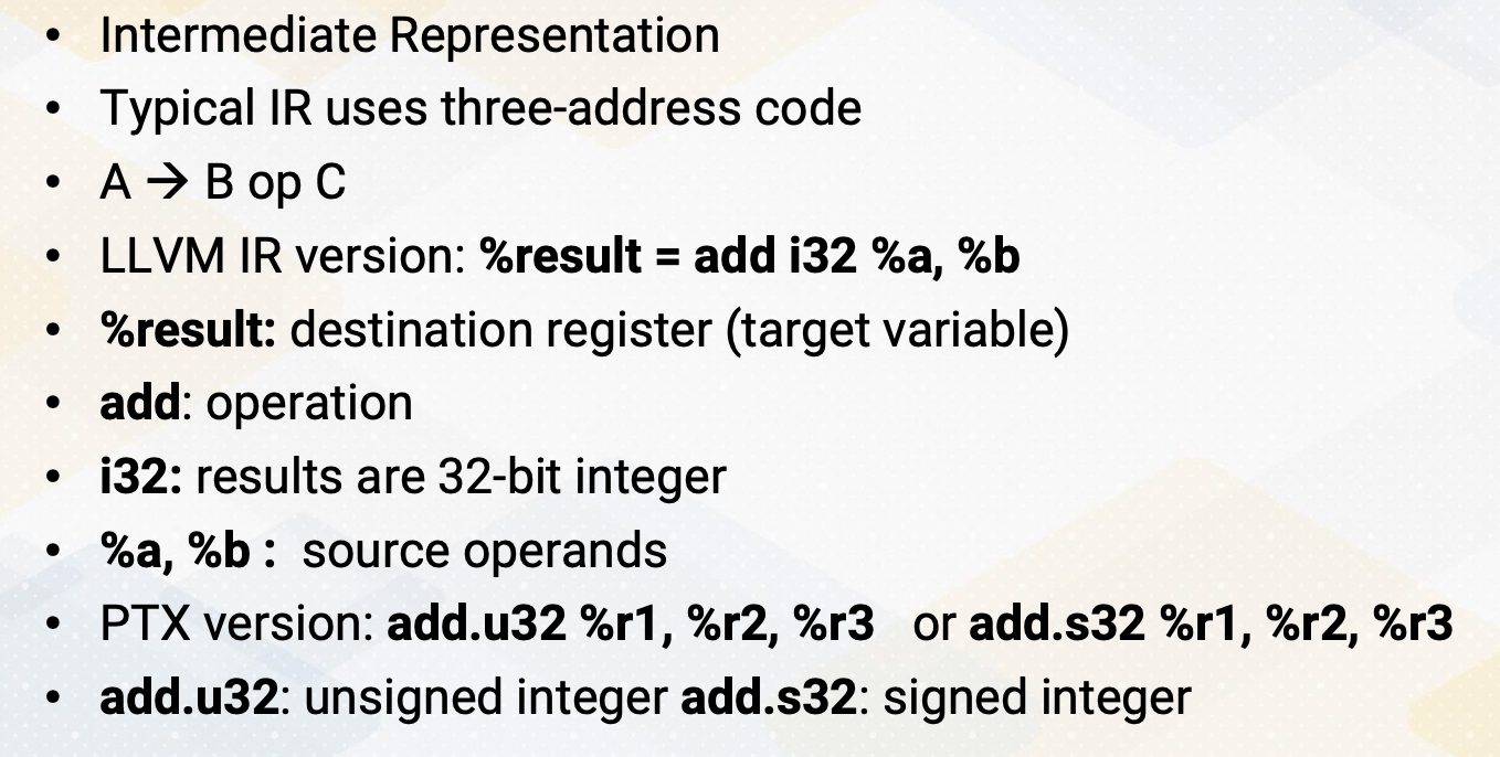
IR, is this an intermediate representation? Typically IR uses three address code such as A equals B op C. The equivalent version of this code in LLVM IR is %result = add i32 %a, %b. %result indicates a destination register and then also target variable. Add is an operation, and i32 indicates that the result of this instruction is 32 bit integer. And a and b indicate source operands. The corresponding PTX IR version will be add u32, r1, r2, r3 or add 32, r1, r2, r3 because PTX has a separate add for unsigned integer and also signed integer.
Basic block
What is basic block? Basic block is a maximum sequence of instruction streams within one entry and one exit. Since it has only one entry, only the first instruction in a basic block can be reached from outside. And since it has only one exit, once the program enters a basic block, all instructions inside a basic block needs to be executed. Typically, all instructions are consecutively executed. And it is also common that exit instruction is a control flow instruction.
One thing to note is optimizations within a basic block is typically local code optimization because it doesn’t know outside of basic block and it optimizes the best it can do within a basic block scope.
Flow graph
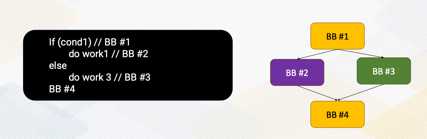
Let’s look at an example of flow graph. In the flow graph, each node represents a basic block, and path indicates possible program execution path. A program typically has entry node, this is the first statement of the program. Here, if else statement that we have seen so far, in many cases, this if else statement will generate the following control flow graph.
Example of if-else PTX Code (1)
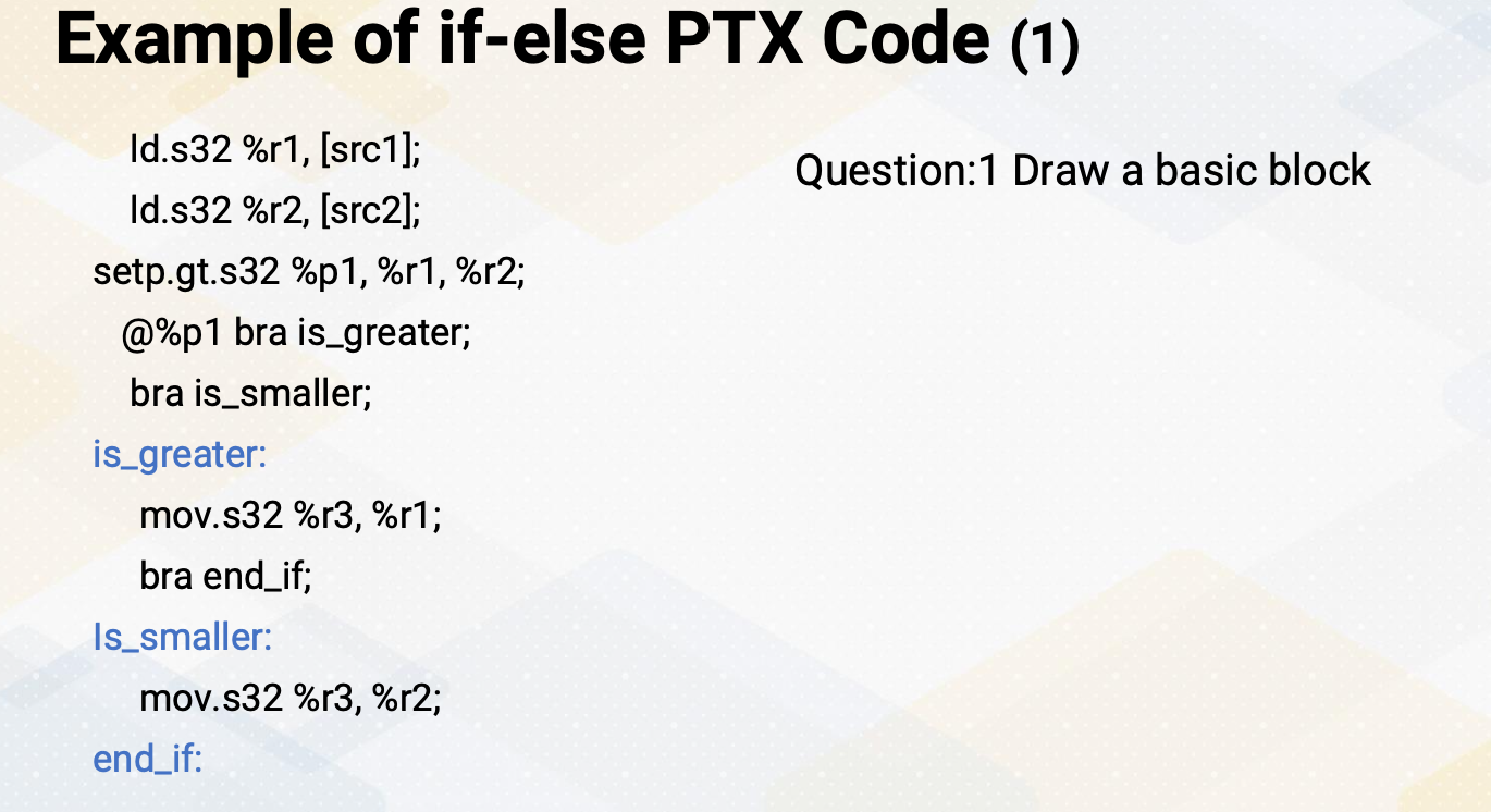
Then let us look a little bit more realistic example in the PTX. Here is an if else code that’s generated for PTX version. First, let’s find the basic block from this example. In this code, blue font indicates labels.
Algorithm to Find Basic Blocks
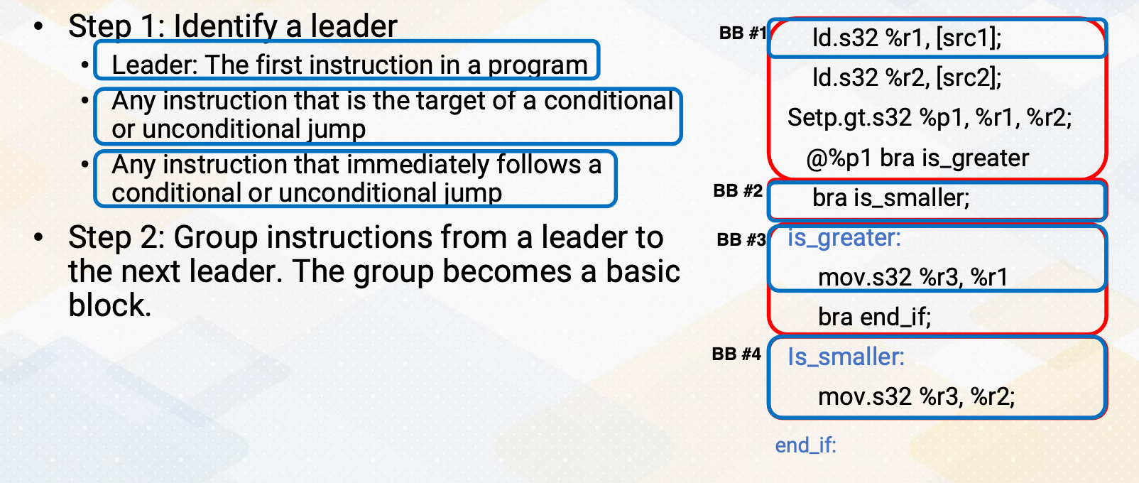
Here is an algorithm to find basic blocks. The first step is identifying a leader. Leader can be the first instruction in a program or any instruction that is the target of a conditional or unconditional jump or any instruction that immediately follows a conditional or unconditional jump. So in this example, first the first ld instruction is the first instruction in the program, so this is a leader. And the second the instruction, the label is_greater, is a target instruction of branch is greater. So this is also leader. And the instruction is_smaller is also target of branch is smaller.
So this is also leader instruction. Since that one of the condition says an instruction that immediately follows condition or unconditional jump is also a leader, this branch is smaller is also leader instruction because there is a branch is greater instruction. In step 2, we group instructions from a leader to the next leader, and then the group becomes a basic block. And here, the basic block 1, here basic block 2, and here basic block 3, and here basic block 4, etc.
Example of if-else PTX Code (2)
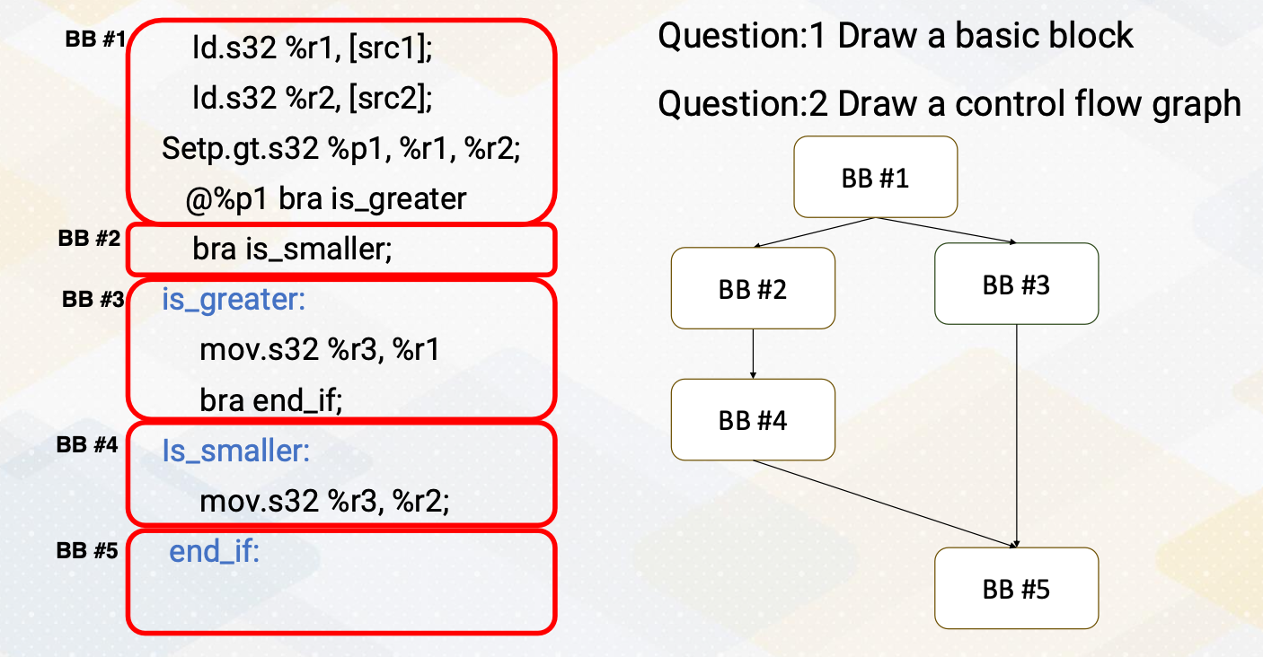
Once we identify a basic block, let’s draw control flow graph. These basic blocks will generate the following control flow graphs. In basic block 1, it has a path to basic block 2 and basic block 3. And basic block 2 has unconditional jump to basic block 4, so it has a path. And basic block 3 has an unconditional jump to basic block 5. Both basic block 3 and basic block 4 means a basic block 5, which is an end_if label code.
In this video, we covered intermediate representation, IR, and its significance. We explored the techniques for identifying and defining basic blocks, and we also demonstrated how to construct a control flow graph.
Module 10 Lesson 4 : Introduction to Data Flow Analysis
Learning Objectives
- Explain global code optimization
- Understand example code optimizations
- Explain the basic concept of data flow analysis
- Explain the concept of reaching definitions
In this video, we study data flow analysis. Throughout this video, the learning objectives are: explaining global code optimization, understanding example code optimizations and also be able to explain the basic concept of data flow analysis. And also to be able to explain the concept of reaching definitions.
Global Code Optimizations
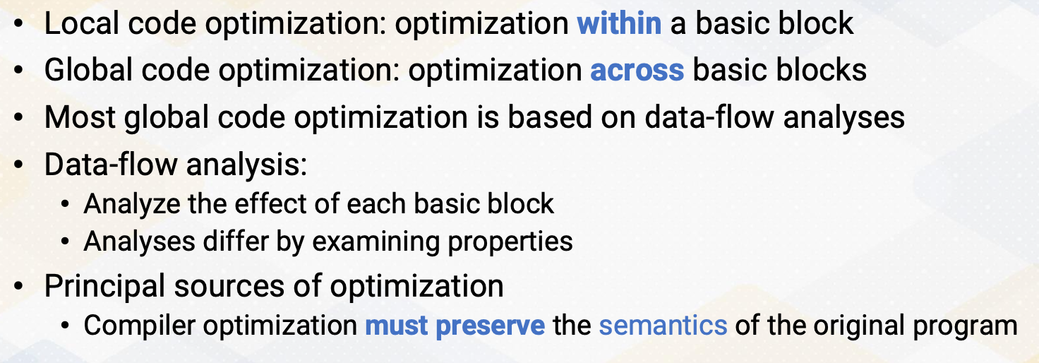
Global code optimizations. Local code optimization is optimization within a basic block. Global code optimization is optimization across basic blocks. And most global code optimization is based on data flow analysis. Since we need to understand how the property changes across basic blocks, we should have some mechanism to understand the property changes and that mechanism is based on data flow analysis. So most global code optimizations are based on data flow analysis. Data flow analysis, analyzes the effect of each basic block and analyses differ by examining properties. Please also note that the principal sources of optimization is compiler optimization must preserve the semantics of the original program. So the behavior of the program should be preserved even after you perform any optimizations. This is very critical to not to change any functionality of a program.
Examples of Code Optimizations
Examples of code optimizations. First, removing redundant instructions. Sometimes there are instructions that are doing the same work, in that case we want to remove such redundant instructions. Copy propagation. It finds constant values and it propagates those constants. And occasionally, after copy propagation we find redundant instructions. Dead code eliminations identifies the code that will never be executed. And so it eliminates such code. And code motions are performed to improve performance, it also detects induction variable because induction variable can have special optimizations and examples could be reduction strength.
Data-Flow Analysis Abstraction
Here, data-flow analysis abstraction. It is an execution of a program and it considers transformation of the program state.
- The input state is program point before the statement and
- output state is program point after the statement.
Transfer Functions
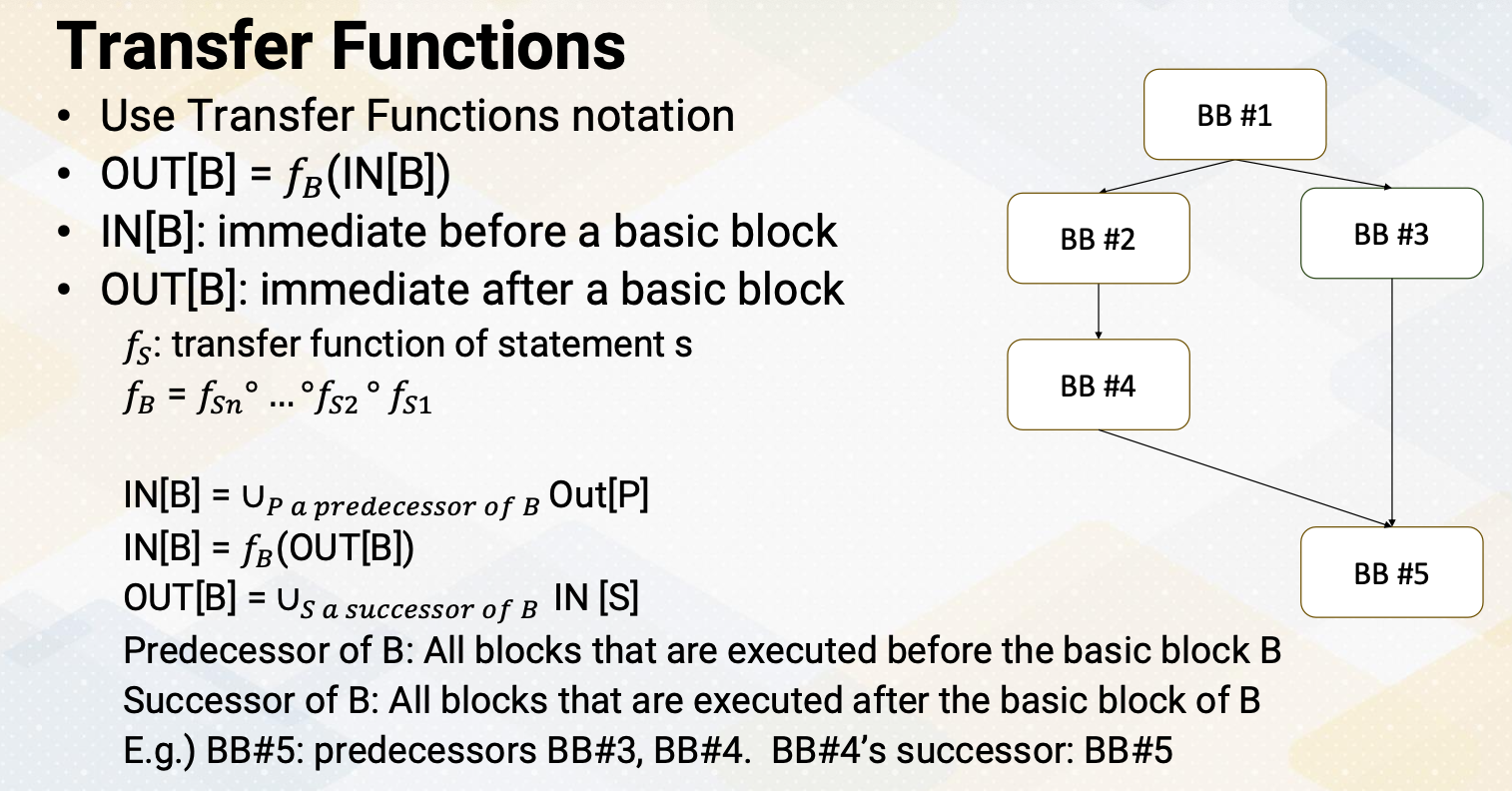
It also uses the transfer function notations. OUT[B] = fB(IN[B]), the IN[B] is immediate before a basic block and OUT[B] is immediate after a basic block. fs is a transfer function of statement s and fB concatenates all these statements within a basic block. So it considers all the instructions inside a basic block. Often IN[B] is union or predecessors of basic block, the output values. So in the case IN[B] can be represented as, IN[B] = fB(OUT[B]) or OUT[B] equals a successor of basic block of IN[S]. Here is an example of control flow graph. Predecessor of basic block B means all blocks that are executed before the basic block B and successor of B is all blocks that are executed after the basic block of B. In this example basic block 5, the predecessors are basic block 3 and 4. And basic block 4 successor is basic block 5. So when you compute in our basic block 5, we should consider all the basic block 3 and basic block 4.
Reaching Definitions
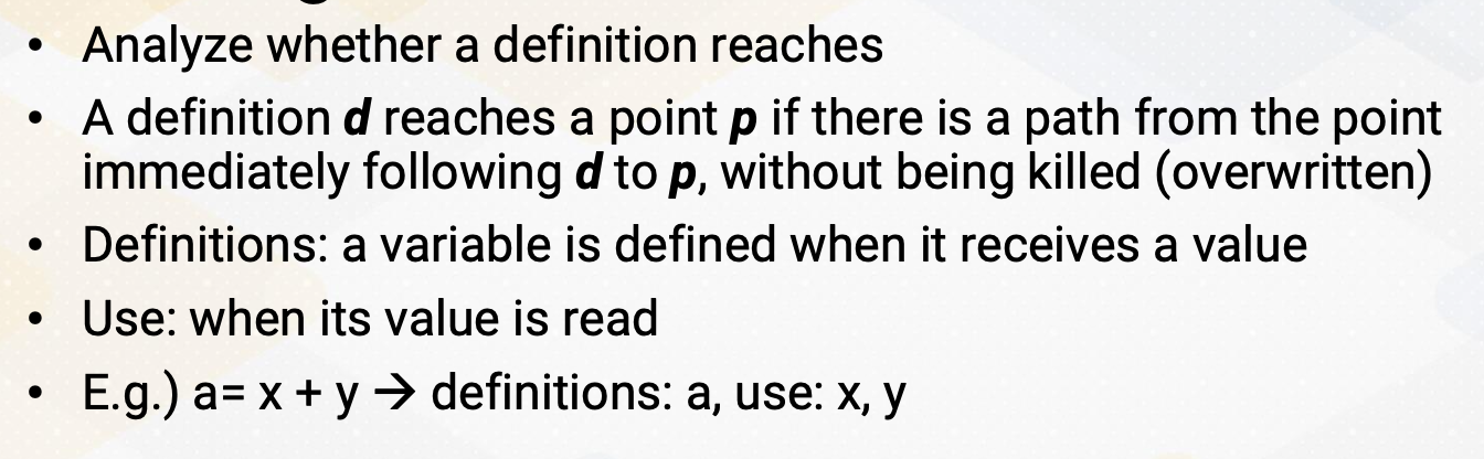
Let’s look at this transfer function a little bit more detail with reaching definitions. Reaching definition analyze whether a definition reaches or not. A definition d reaches a point p if there is a path from the point immediately following d to p without being killed, which means without being overwritten. In definitions, a variable is defined when it receives a value and use means when its value is read. For example, a = x+y and definitions a and uses x and y.
Gen and Kill
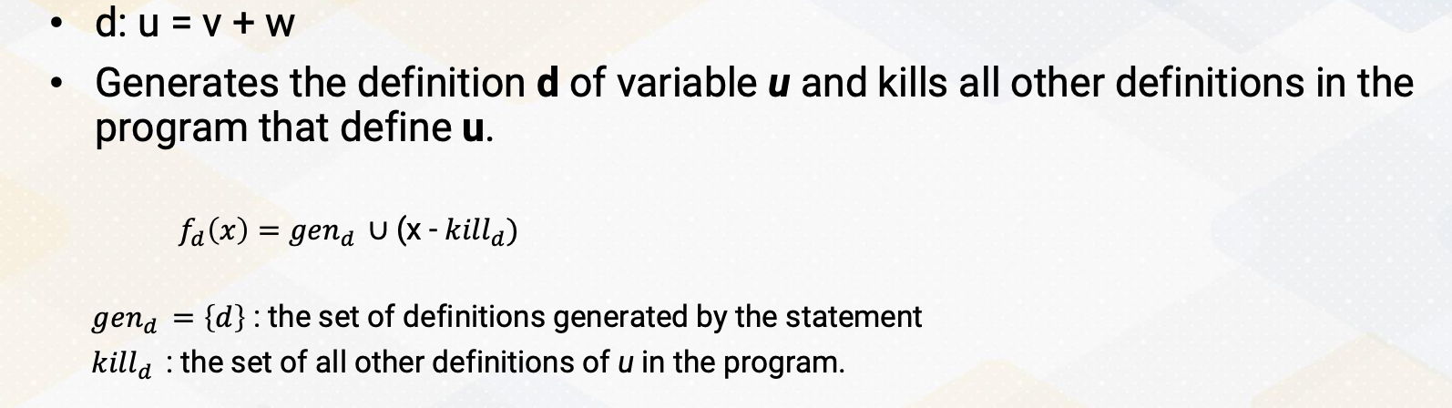
This can be also represented with gen and kill. There is a d statement u = v+w. It generates the definition d of variable u, at the same time it also kills all other definitions in the program that defines u. And with the transfer rotation, fd(x) = gen_d U (x-killd). And gen_d is the set of definitions generated by the statement and then killd is the set of all other definitions of U in the program.
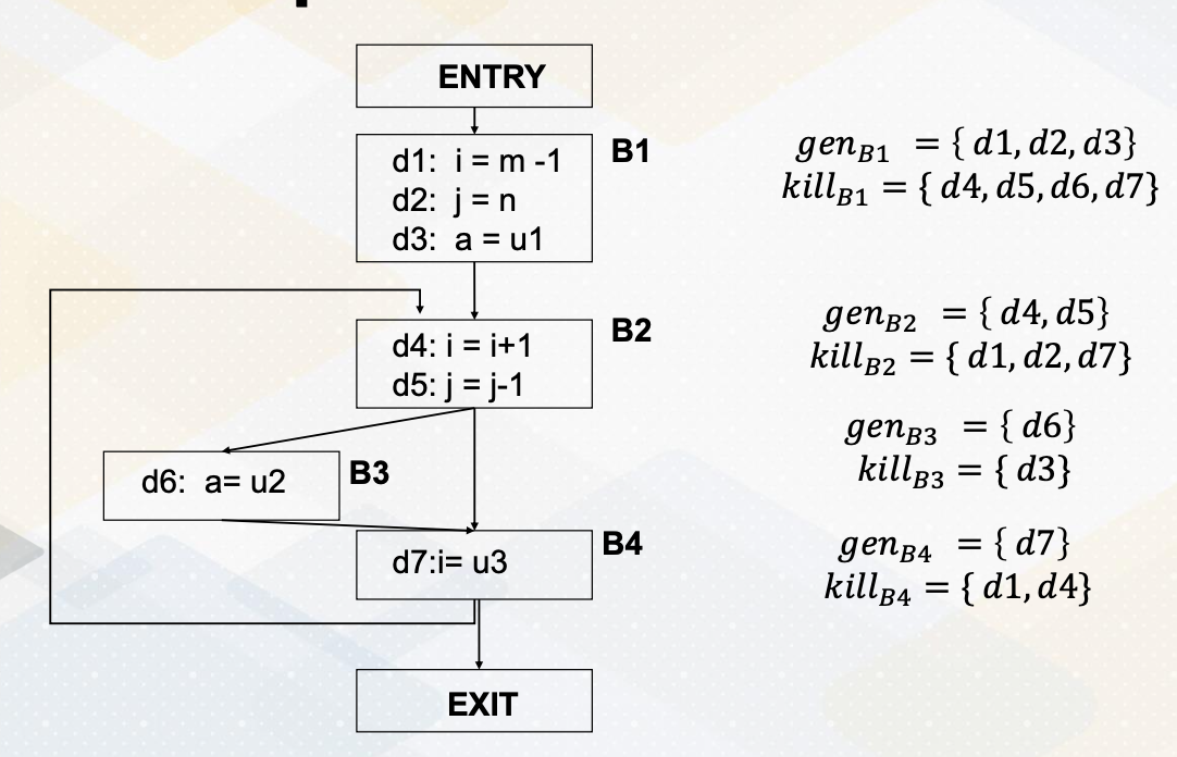
Let’s look at gen and kill set in more detail by looking at this example. It has a entry and it has four basic blocks and exit. Basic block B goes to basic block B2 and basic block B2 can go to basic block 3 or basic block 4. And then basic block B4 goes back to B2 or can exit. Basic block B1 has three statements, B2 has two and B3 has one and B4 has one statement.
First, basic block 1. The gen set is d1, d2, d3 because all these statements generate definitions. It generates definitions for i, j and a, which means it also kills all other definitions in a program that defines i, j, a. In this example, all the rest of the instructions d4, d5, d6, d7 defines one of i, j, a so the basic block 1 kills all other statement d4, 5, 6, 7. In basic block B2, it defines d4 and d5, which generates definition for i, and j. Again, that means it kills definitions of i, and j in the program, d1, d2, and also d7. Basic block 3 generates definition in the statement d6, which generates definition of a, so then it also kills definition of a in other part of the program which is d3. In basic block 4, similarly, it generates definition for d7 which is an i, so that it kills definition of other statement that defines i, which is d1 and d4.
Generalized Transfer Functions
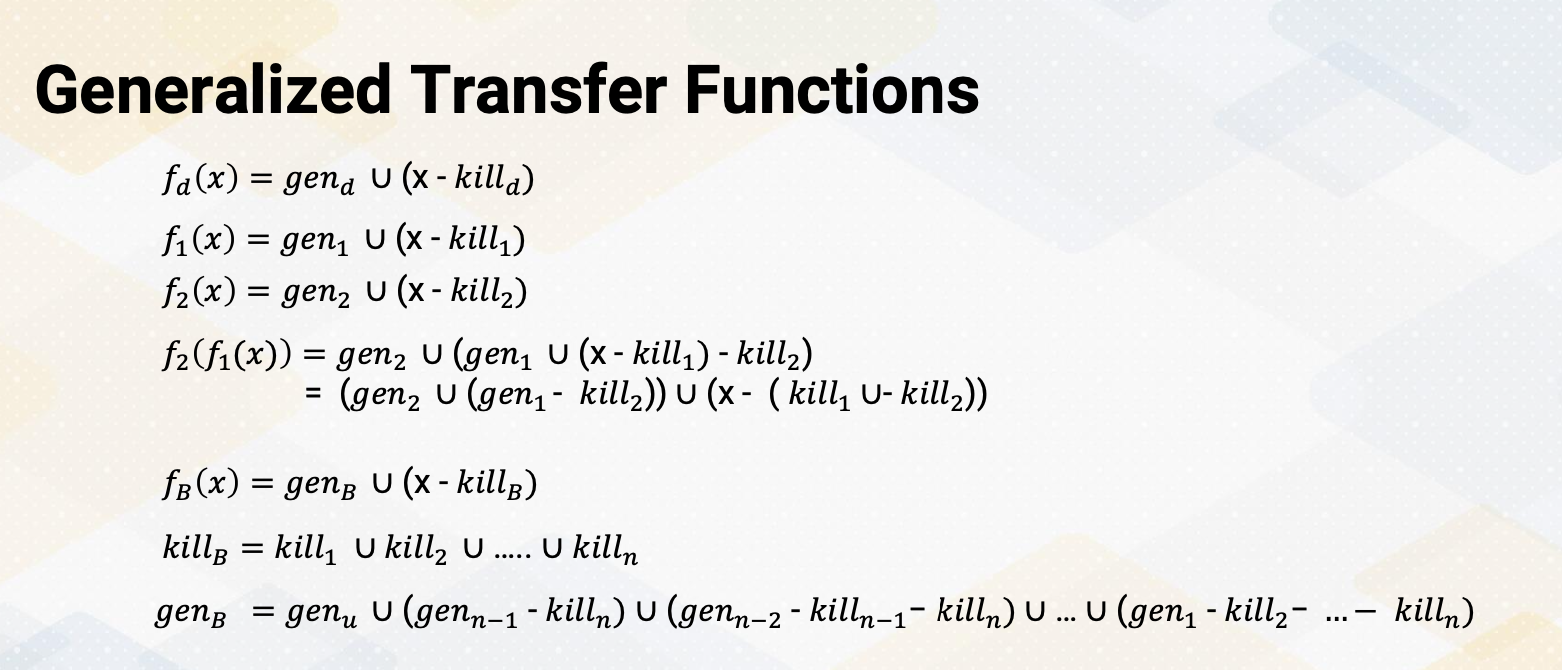
By having gen and kill set, we can apply these transfer functions to compute reaching definitions. We can first compute reaching definition for basic block 1, propagate the basic block 2. and then so on, so then we can generalize fB(x) = gen_B U(x-killB). And then killB is union of all the kill sets and genB is union of the previous basic blocks precessors. We will look at a more detailed example of this using transfer functions in next video.
In this video, we studied that global code optimization involves analyzing code across basic blocks. We saw that data flow analysis relies on transfer functions. We use reaching definitions within data flow analysis to illustrate an example.
Module 10 Lesson 5 : Example of Reaching Definitions
Learning Objectives
- Apply transfer functions for reaching definitions analysis
- Explore an example of reaching definitions in control flow analysis
In this video, we review the reaching definitions with an example. Here we apply the transfer functions to perform the reaching definition analysis. We will also explore an example of reaching definitions in the context of control flow analysis.
Continue the Example of Reaching Definitions
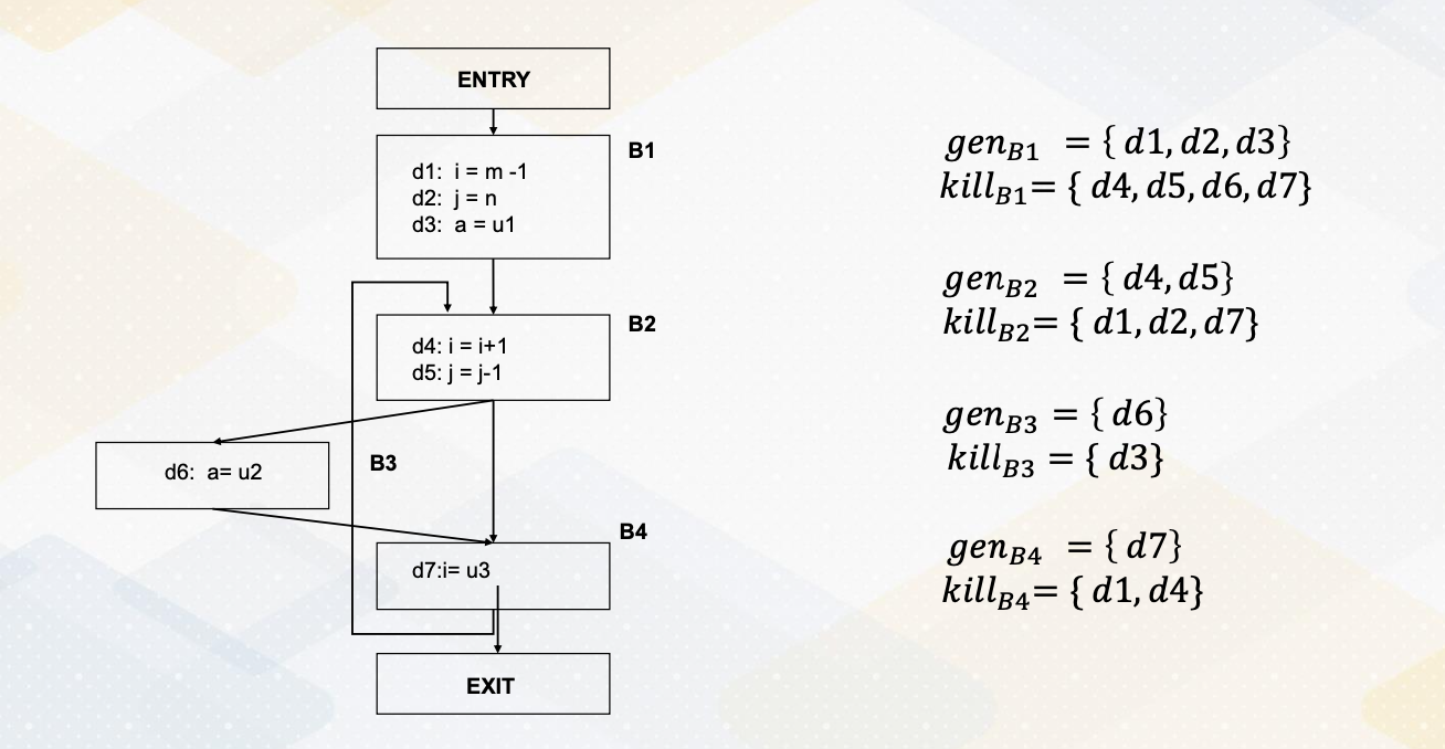
Let’s continue the example of reaching definitions. In the previous video, we have created gen and kill set for each basic block. As a reminder, gen is the set of definitions generated by the statement in the basic block and the kill is the set of all other definitions of the corresponding variables in the basic block. So here we get basic block 1’s gen and kill set and we have a basic block 2’s gen and kill set and basic block 3 and 4 so on.
Control Flow Equations
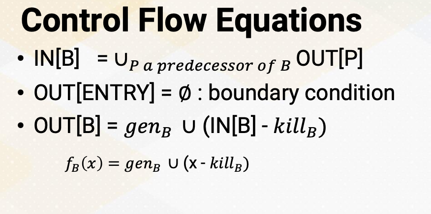
In the control flow equations for reaching definitions, IN(B) is a union of all predecessors of out blocks. As a boundary condition, the entry of out is empty. With IN, the out of each basic block is IN minus the kill set in the corresponding basic block and then the union of genB set. Hence, the transfer function is fB(x) equals genB U ( x minus killB).
Algorithm
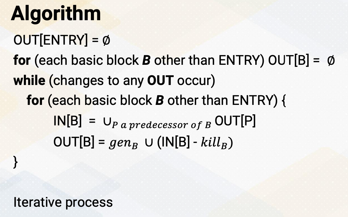
To compute this transfer function, the compiler implements the algorithm using an iterative process. First, we initialize out [ENTRY] as an empty set. For each basic block B, we also initialize Out[B] as null. In the iterative process, we go through each basic block. First we compute IN[B] by combining the out values of all predecessor blocks, then OUT[B] is computed using the transfer functions. Once we have processed all the basic blocks, we check for any changes in the OUT values. If there are changes, the iteration continues until none of the OUT values change.
Illustration of Reaching Definitions
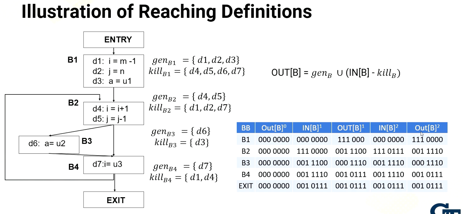
Here is an example. First, all OUT[B] is initialized with zero and where each zero indicates the value of d1 to d7 as a 7-bit value. And here, this superscript indicates iterations. So here it shows the iterative initialization values and iterative 1s and iterative 2s. Let’s start going through from the basic block 1. The basic block 1, the predecessor of basic block is entry and so the out of entry is zero, so IN[B] is also all zeros. And then OUT[B] is genB U (IN[B] - killB) so the kill set of B1 is d4, 5, 6, 7, but since IN is zero, this remain zero. And the union is a gen d1, d2, d3. So d1, d2, d3 values set is 111 and we have a 000. So this is out value for basic block 1. And now let’s move to the basic block 2. Basic block 2 has the predecessors of B1 and also B4. So the union of out of B1 and B4. Here the B4 is still zeros, but out of B1 is 1110 so union which is actually the sum becomes 111 and 0000. And then from here we have the kill. The kill d1, d2, d7. So d1, d2 value will be cleared and then there is a gen which you need to get union value d4 and d5. So d4 and d5 value becomes 11. So the OUT B2 becomes 0011100. Now let’s move to the basic block 3. In the basic block 3, the predecessor is only basic block B2. So B3’s IN value is same as B2 OUT which is 001 1100. From here we have to subtract the kill which is d3, so d3 will get cleared. And then we add d6. So we set d6 6 bit as one. So OUT B3 becomes 000 1110. Let’s move to the basic block 4. Basic block 4s predecessors are B3 and B2. So union of OUT B2 and B3, 001 1110 is IN of the B4. And here we subtract the kill d1 and d4. So we clear d1 which was already zero and d4. And then we add gen d7, so 7 bit becomes 1, so the final value is 001 01111. And then exit.
The exit block, the predecessor is only B4 so OUT of B4 001 01111 becomes IN. And exit block does not have any gen and kill set, so OUT value is the same as IN. So this is the end of the first iteration, and obviously the values are changed from the zero, the initialization value. So we have to go through the next iteration. So we start from again basic block 1. The basic block 1’s input is the output of entry is still 000. That OUT of B1 is the same as the previous iteration, 111 000 and the basic block B2 the predecessors are B1 and B4, so union of OUT B1 and B4. So union of B1 and then there is B4’s OUT value now has values. So union of these values B4’s OUT and B1s are combined, becomes IN of B2 which becomes 111 and 0111. 111 comes from here, B4’s OUT. And that becomes IN of B2. Again, here we subtract the kill set, d1, d2, d7, so d1, d2, d7 got cleared and then we add d4 and d5. So fourth value becomes 1 and 5 was already 1. So OUT of B2 becomes 001 1110. And then we move to B3, the B3’s predecessor is only B2, so the IN value is same as B2’s OUT 001 1110 and then here again, we clear d3 because a kill set, and then 1 becomes 0. And then we add d6, the gen. So we add the 1 which was already 1 so our value of B3 becomes 000 1110. And then we move to the basic block 4, the basic block 4’s predecessors are B3 and B2. So union of these OUT values, B2 and B3 becomes the IN value, so 001 1110. Which happened to be the same as the previous iteration, so OUT value will be the same as the previous iterations, 001 01111, then exit value is the IN value will be the same as the OUT B4. And then OUT exit value will be also the same. This is end of the second iteration. Although we did not show the third iteration, if you repeat this process, the OUT value remains the same. So this will end this iterative process.So this is showing an example how we can compute the reaching definitions with the iterative algorithm.
So here in this video, we apply the iterative algorithm to find reaching definitions and review the algorithms. First, we compute the gen and kill set for each basic block and identify predecessors of each basic block. Then we apply the transfer function to all basic blocks and then the iterative process starts when there are no changes in the OUT for all basic blocks. <!– <iframe class=”embed-video” loading=”lazy” src=”https://www.youtube.com/embed/10oQMHadGos” title=”YouTube video player” frameborder=”0” allow=”accelerometer; autoplay; clipboard-write; encrypted-media; gyroscope; picture-in-picture” allowfullscreen
</iframe> –>
Module 11: Compiler Background - II
Objectives
- Be able to explain comparisons with other GPU programming
Required Readings:
- OpenCL overview
Module 11 Lesson 1 : Live-Variable Analysis
Learning Objectives
- Explain the concept of Liveness Analysis
- Explore the application of Liveness Analysis in register allocation
- Identify data-flow equations and explain their role in analysis
In this module, we’ll continue on compiler backgrounds. Here are learning objectives. In this video, we want to explain the concept of liveness analysis. We also want to explore the application of liveness analysis in register allocation. We’ll also identify data flow equations and explain their role in analysis.
Live-Variable (Liveness) Analysis
- Liveness analysis helps determine which variables are live (in use) at various program points.
- Usage: register allocation. Register is allocated only for live variables, ensuring registers are allocated only to live variables.
Liveness analysis is a critical technique used to identify which variables remain in use at different program points during code execution. One of its key applications is in the field of register allocation. When allocating registers, liveness analysis ensures that registers are reserved exclusively for variables that are actively in use at a given point in the program. This approach optimizes register spills. so it enhances overall program performance.
Data-Flow Equations
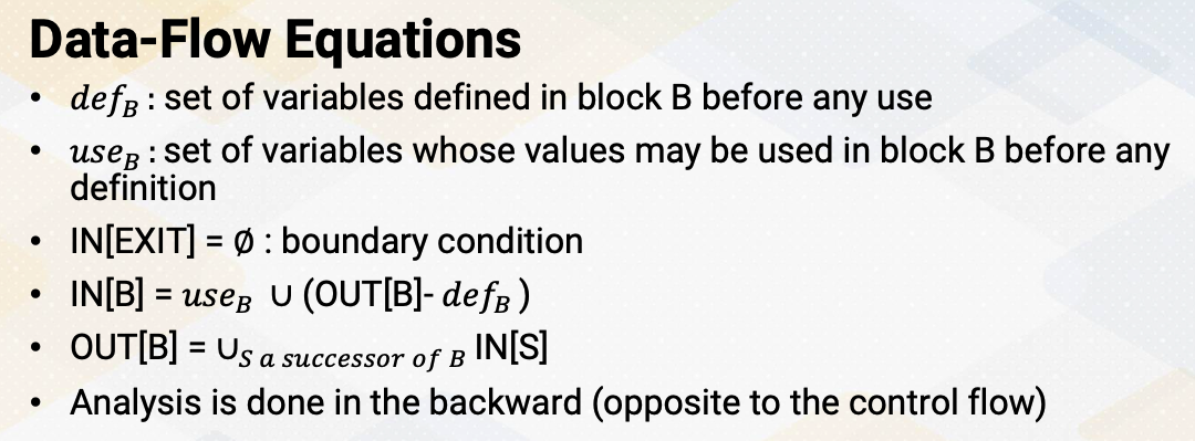
Let’s look at data flow equations, defB is a set of variables defined in block B before any use. useB is set of variables whose values may be used in block B before any definition. IN[EXIT] is a boundary condition, it specifies the boundary which means there’s no variables alive on exit from the program. IN[B] = useB union (OUT[B]-defB) says that a variable is live, coming into a block if either it is used before redefinition in the block or it is coming out of the block and is not redefined in the block. OUT[B] is a successor of block’s IN values. It says the variable is live coming out of block if and only if it is live coming into one of its successors. And this analysis is done in the backward which is opposite from the reaching definition analysis.
Algorithm
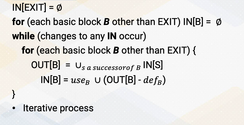
Let’s look at the algorithm. First, we initialize EXIT IN value as 0. And we also initialize all the IN values as 0 other than EXIT. Then we’ll start iterative process until there’s no changes in value. Within an iterative process, we go to the full loops. The full loops go through each basic block. OUT[B] is IN values of any successor of basic block B. Then we combine all the values. The IN[B] = useB U (OUT[B]-defB). And then we iterate process.
Example of Live-Variable Analysis
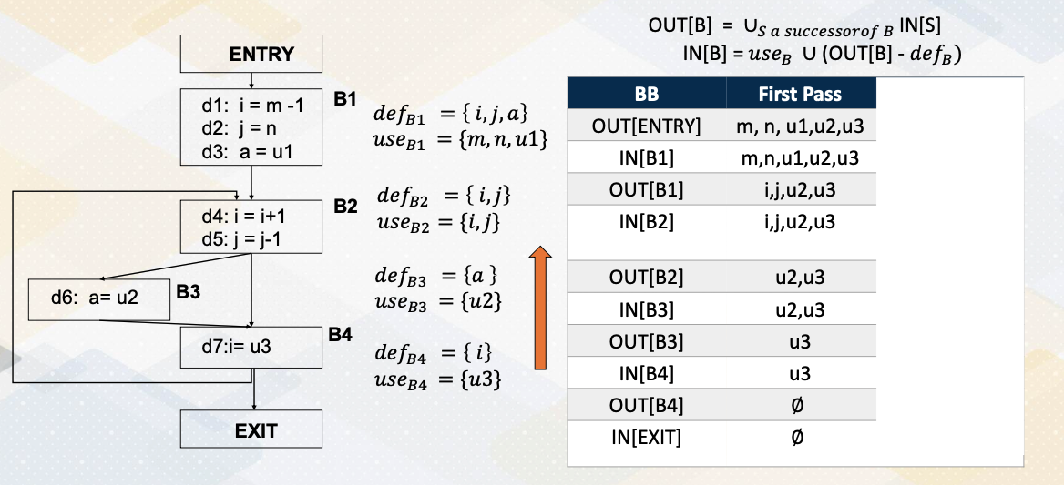
Let’s look at an example for the live variable analysis. We have the same control flow graph that we saw in the previous example. First, let’s compute the def and use set. For the basic block B1, basic block B1 defines variables i, j, a. So that is a def set. And also use m, n, u1. So that’s a use set. So reading values becomes a use set and the writing values become the def set. In basic block B2, we define i, n, j, we also use i, n, j. So i, n, j are used and redefined inside basic block B2. And B3 use u2 and it defines value a. So def set is a, use set is u2. In basic block 4 use u3 and then it defines i value. So so def is i and use is u3. Now we go through this liveness analysis, which is the backward process. First we initialize IN EXIT as 0 and OUT B4 as also 0. Then IN B4 is OUT B4-def before union B4. Since OUT B4 is 0 and definition doesn’t subtract any value and then we compute union use B4, so IN B4 becomes u3. Then we move to the basic block 3. basic block 3 has successors before, so OUT B4 is union of successors, so the B4’s input becomes OUT B3, so it’ll be the same value. And IN B3, the first OUT B- def. So u3-def in the basic block 3 is A, so u3 becomes u3. And then union of use B3 which is u2, so union of u2 and u3 becomes IN B3. And then now we move on to basic block B2. B2 has two successors, B3 and B4. So OUT of B2 is union of IN B3 and IN B4, so u2 and u3 and u3 union becomes OUT B2, same as u2 and u3.
And then we compute IN B2, first we compute OUT B-def, so u2, u3-def is i, j. And then we union i, j, so IN B2 becomes i, j, u2, and u3. So let’s move on to the basic block B1. B1 has only one successor B2, so OUT B1 is the same as IN B2, so i, j, u2, and u3. And now let’s compute IN B1. From the OUT B1, we subtract the def i, j, a and then we add use m, n, u1. So we subtract i, a, j and then we add m, n, u1, so final value of IN B1 becomes m, n, u1, u2, and u3. Then OUT ENTRY, because entry of successor is only B1, the same as IN B1. This end the first pass, and then we repeat the same process for the second pass. Again repeat the same, starting from the backward, the OUT B4, the B4’s successor. The B4’s successor is B2. So IN B2’s values becomes OUT B4, so i, j, u2, u3 becomes OUT B4. And then based on this i, j, u2, u3-def_B4 is we eliminate i, and then we add u3, the use value, so the value becomes j, u2, and u3. That becomes IN B4. And then for the B3, the successor is only B4, so IN B4 becomes same as OUT B3. And then we subtract a and then we add u2 so that we get same value j, u2, and u3. And B2 have two successor, B3 and B4. So we have a union of B2 and B3 IN values. So B3’s and B4’s values successors are combined and then becomes OUT B2, j, u2, and u3. Based on that, we also compute IN again, now we subtract defB2 and then add use here, because def and use are the same, the value becomes the same. And then we move on to this OUT B1. The B1’s successor is only B2, so OUT B1 is same as IN B2. At this moment, our values are the same as the first pass, so the second pass IN B1 becomes the same as first pass and then OUT ENTRY value will be the same. Third pass will show the same value as second pass, so iterative process will end after third pass.
Register Allocations and Live-Variable Analysis
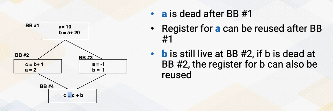
So using these live variable analysis, we can decide when we allocate registers. Here shows an example. These A values are used here defined here and then redefine basic block B2 and B3. So register for a will not be reused after the basic block B1 so that we can reuse variable a’s registers for something else. In the other case, B is still live at basic block B2, so we have to keep the register for variable B. If B is also dead, then we can also reuse the register value for B. So that’s the usefulness of live variable analysis.
Register Allocations
So register allocations for the purpose is only live variables needs to have registers. This means that the compiler allocate registers to variables that are actively used in a specific program section. Sometimes and actually most of the time, there aren’t enough registers available to accommodate all live variables. So the compiler needs to perform registers, spills, and fills. So it temporarily stores values in the memory stack to free up registers for other variables. It’s important to note that PTX assumes an infinite number of registers, which is to simplify the process, therefore, stack operations are not shown in the PTX code.
Summary of Data-Flow Analysis
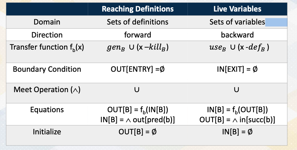
Here is a summary of data flow analysis. The domain of reaching definition is set of definitions and domain of live variable is set of variables. Analysis directions for reaching definition is forward and live variables are backward. Here is transfer functions for the reaching definition genB union x-killB and for live variable useB union x-defB. Both share very similar transfer functions. Instead of using a gen kill set in live variables, you use use and def set. The boundary conditions for reaching definitions is initializing OUT ENTRY, whereas in live variable initialize IN EXIT. That’s because the direction of analysis is one is forward and the other is backward. Both of the meet operations when control flowers are meet are using a union set, and this is another representation of equations and initializations. So in this video, we study data follow analysis for live variable analysis. As a recap, reaching definition analysis uses forward analysis, but live variable analysis uses backward analysis.
Module 11 Lesson 2 : SSA
Learning Objectives
- Explain the concept of SSA (Static Single-Assignment) form
- Explore the basics of converting code to SSA form
- Explain how to merge values from different paths
In this video, let’s learn SSA in more detail. Throughout this video, we should be able to explain the concept of SSA, static single-assignment form. We’ll also explore the basics of converting code to SSA form, and we also discuss how to merge values from different paths.
SSA
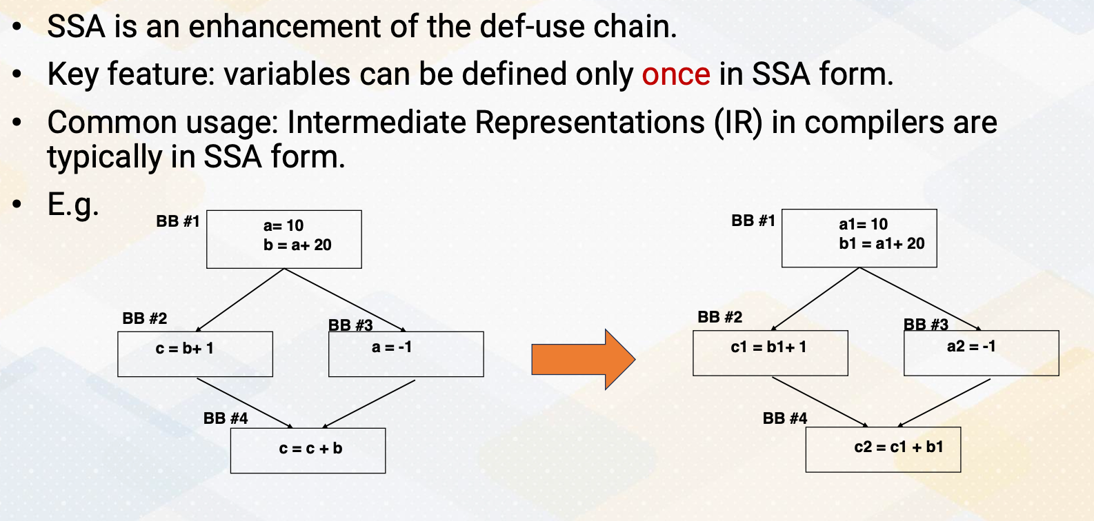
SSA, or static single-assignment, is a form used in compiler optimization and intermediate representations IRs that improves upon the traditional def use chain. One of the fundamental characteristics of SSA is that each variable is assigned a unique definition point, meaning it can only be defined once within the program. This property simplifies analysis and optimizations as it eliminates the need to track multiple definitions of the same variable. Compiler designers often use SSA form as the basic for their intermediate representations because it provides a structured and efficient way to represent program information. This form simplifies various compiler optimization passes. Here in this example, we have a and b, and c. And throughout the SSA forms, they will receive a1, a2, b1 and c1 and c2. So there will be new versions whenever there is new definitions.
SSA and Control Flow Graphs
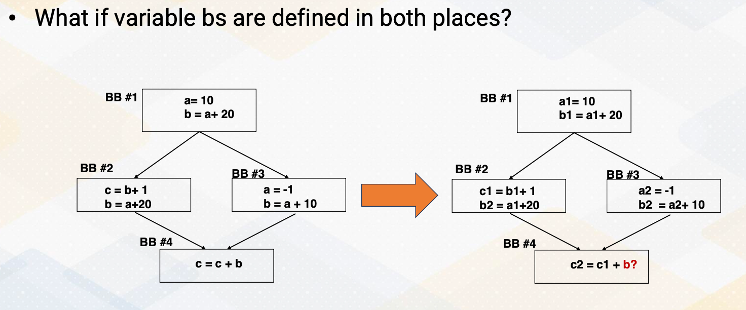
One challenge is what if the variable bs are defined in both places? In this example, the variable bs are defined in basic block b2 and b3 and basic block 4 is using variable b, where we don’t know which one will be used, and this will be decided at one time.
Phi functions
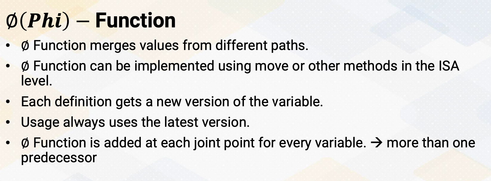
To solve this problem, Phi function is defined in SSA. The Phi function is probably the most intelligent and interesting part of SSA. The Phi function merges values from different paths. Phi function can be implemented using move or other method in the ISA level such as select or conditional move. And each definition gets a new version of the variable, and the usage always use the latest version and the Phi function is added at each joint point for every variable and when there are more than one predecessors.
SSA Conversion Example
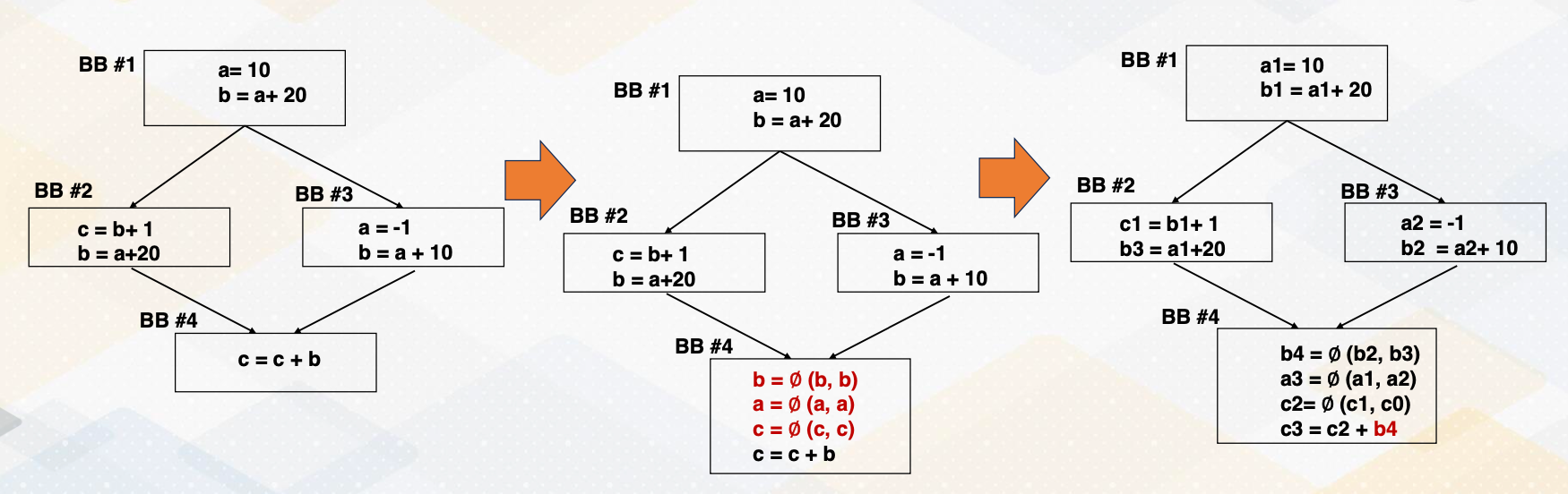
Now with the Phi function, let’s convert this control flow graph with SSA form. First, we insert Phi functions for the variable b, a, and c because b are defined in both places, a are defined and c has only definition in only one path. and each of the definition will receive the new versions, a1, b1, a2, b2, and c1 and b3. Phi functions combine the variables in the both paths and b2 and b3 or in a1 which comes from this path or a2 which is redefined in the basic block 3. And c2 is also combined in c1, or if it comes from this path, the original definition of c0 will be used. And after that, the c3 use b4 which is newly defined in this basic block.
When to Insert ∅ Function ?
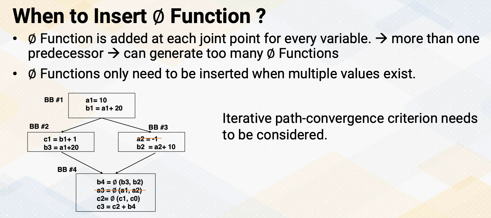
Then the question becomes when to insert the Phi functions? The Phi function is added at each joint point for every variable. But if we do that, it might generate too many Phi functions. We only want to add Phi functions if there are multiple values exist on the path. To do so, iterative path convergence criterion is needed to solve this problem. In this example, if a2 definition is not here in basic block 3, then we don’t also need to have Phi function for a3. So we want to know when we don’t need to insert these Phi functions.
Path-Convergence Criterion
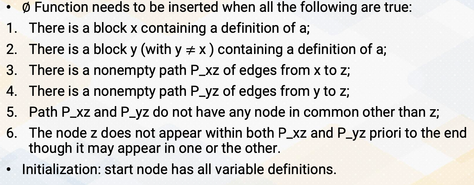
Path-convergence criterion is Phi function needs to be inserted when all the followings are true. First, there is a block x containing a definition of a. And second, there is a block y, y is not equal to x containing a definition of a. And there should be a non empty path, edges from x to z. And also non empty path from y to z and this path x to z and path y to z do not have any node in common other than z. Node z might appear other places, but it should not appear prior to P_xz and P_yz. So first, we initialize the start node have all variable definitions.
Applying Path-Convergence Criterion
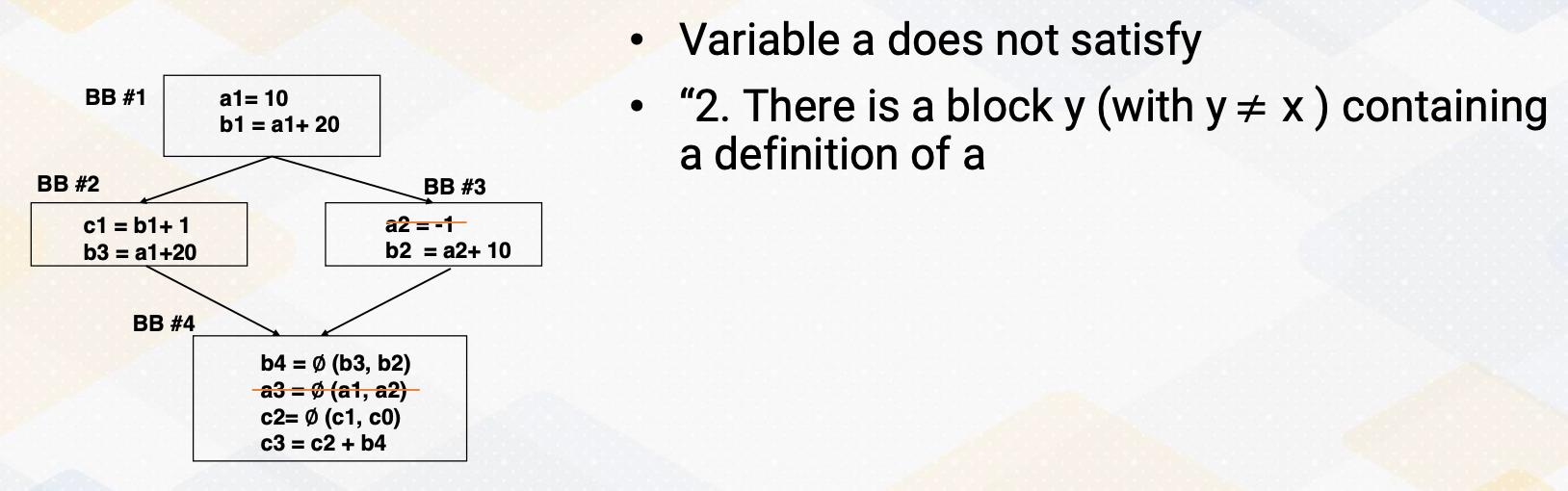
And if you use these path convergence criterions , and variable a, there is no block that contains the definition of variable a from path b1 to b4 because there is no definition of b2 and b3. If we assume a2 = -1 doesn’t exist, so then we can say we remove this Phi function.
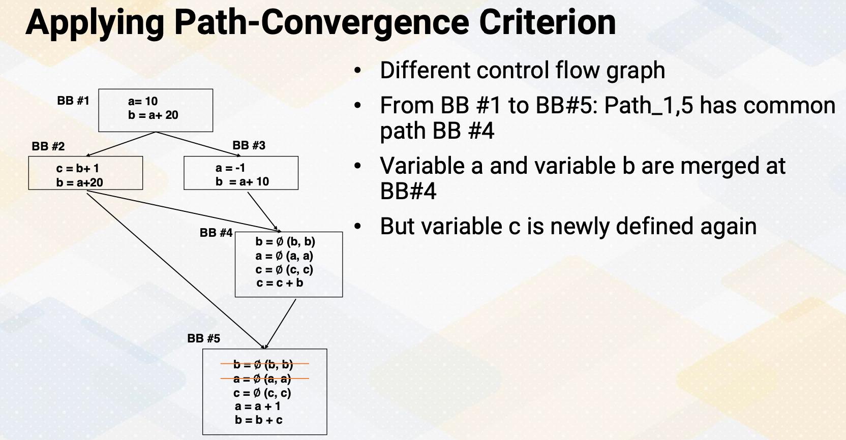
But let’s look at a little bit different control flow graph which is similar. So first, there is a path for this b and a, so that we insert the Phi functions of a, b, c in the basic block 4. But because when it comes from b1 to b5 or b5 through the b3, there is a common path in basic block 4. So because of this common path insert Phi functions in here. So then from here to here, we do not need to insert basic blocks for a, b, c. But because c is new defined, we need to keep the Phi function for the c and b defined basic block 2 is merged here. So we don’t also need to insert Phi function.
∅ Function in LLVM
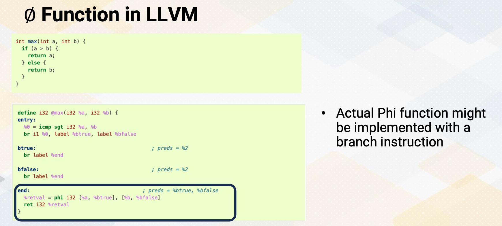
And let’s look at Phi function in LLVM here. This if max function, if else and this is converted SSA form and these SSA form, these Phi functions are also used in the Phi function, the name, literally in LLMV as well. So LLMV treated Phi functions as the same definition of SSA. And back up the ISA, this Phi function will be converted back to if else statement or conditional move depending on the ISA. Here’s a summary. SSA, static single-assignment form enhances SSA data follow analysis by allowing variables to be defined only once. The Phi function is used to merge values from different paths in SSA form. The path convergence criterion helps decide when to insert Phi function during SSA conversion. SSA form simplifies data flow analysis and enables more effective optimizations.
Module 11 Lesson 3 : Examples of Compiler Optimizations
Learning Objectives
- Explain the fundamental concepts of compiler optimizations
- Explore specific optimization techniques, including Loop Unrolling, Function Inlining, and more
In this video, we’ll study examples of compiler optimizations. Here we will cover the following learning objectives. First, we’ll explain the fundamental concepts of compiler optimizations, and second, we’ll explore specific optimization techniques such as loop unrolling, function inlining, and more. And by the end of this video, you should have a clear understanding of these topics.
Loop Unrolling
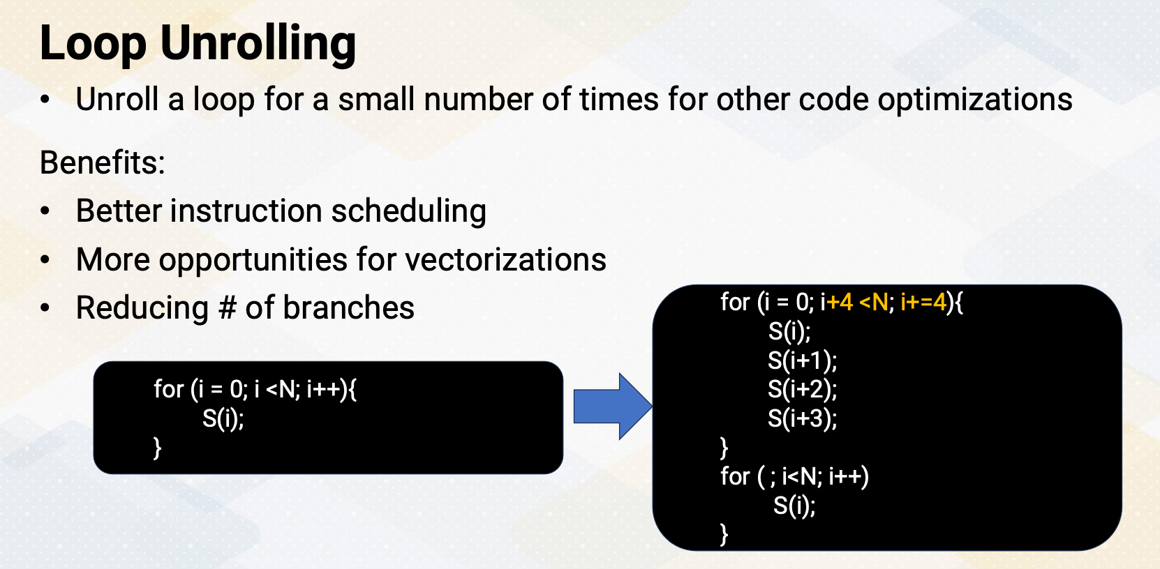
Loop unrolling is a technique where loop is manually or automatically expanded to execute its iteration for a small number of times. This optimization offers several benefits, including improved instruction scheduling, increased opportunities for vectorization, and also a reduction in the number of branches in the code. Here is an example. The for loop contains a statement for each loop iteration. And then through the loop unrolling, instead of incrementing the loop by one iteration, it increments by four, which is unrolling the loop by a factor of four. Additionally, there is an epilog loop for remaining loop iterations if a loop needs to be iterated more than a multiple of four.
Function Inlining
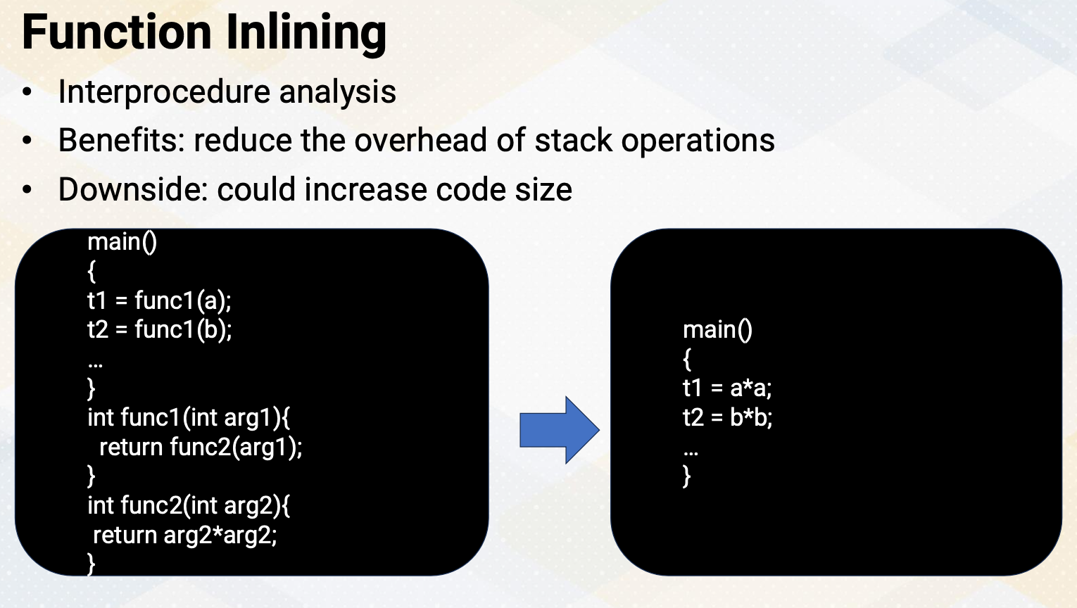
Function inlining is a compiler optimization that replaces function calls with the actual function code. It reduces stack operations overhead and also it might introduce more compiler optimizations. It is an inter-procedure analysis, so it is one of the global optimizations. However, it might increase code size due to duplicated code. So we have to be very careful when we perform function inlining or not. For example, in this code, the left code shows two functions, func1 and func2. And instead of calling these two functions, t1 and t2 can be simply computed with aa and bb.
Dead Code Elimination
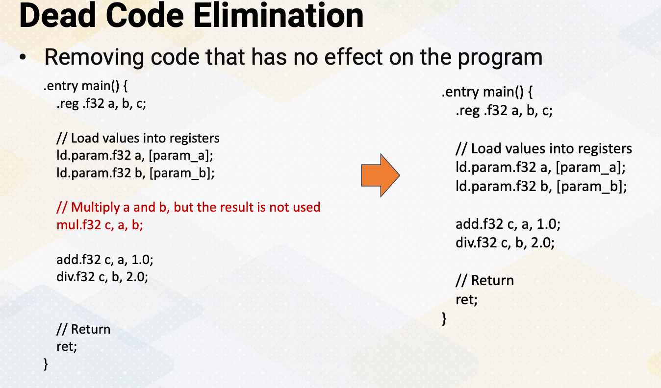
Dead code elimination is a process that identifies and removes instructions which doesn’t contain the fine output of a program. This optimization helps reduce the size of the code and potentially improve execution speed. Here is a simple example of PTX dead code elimination. The code example shows that the red font indicates the code that will be eliminated. Here, mul.f32 c, a, b and c values will not be reused, so it can be safely removed. as shown in the right side.
Constant Propagation
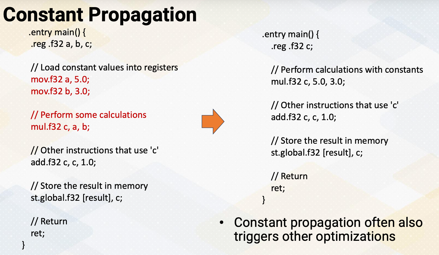
Constant propagation is an optimization technique that replaces variables with their constant values in the code, eliminating unnecessary variable access. Here’s another example of PTX code that demonstrates constant propagation. Instead of passing a and b, we can replace this value 5.0 and 3.0. Constant propagation often also triggers other optimizations. So mul.f32 c, 5.0, 3.0. could also be replaced with simply 15 and this constant can be propagated through the entire program.
Strength Redunction
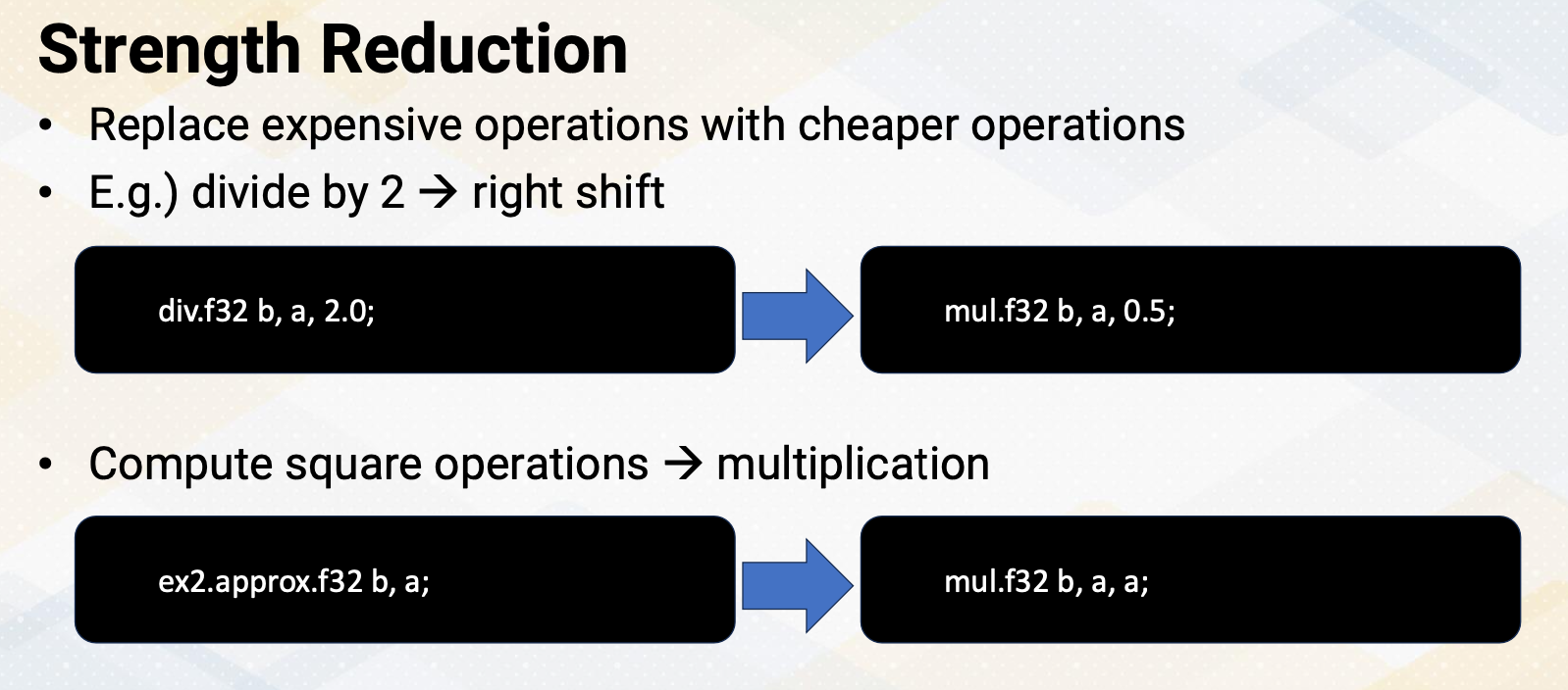
Strength reduction is an optimization technique that involves replacing expensive operations with the cheaper ones. One common example of strength reduction is replacing the operation divided by 2 with more efficient operations such as right shift. Another example of strength reduction is replacing costly square operations with more efficient multiplication operations as shown in this example.
Code Motion: Loop-Invariant Instructions
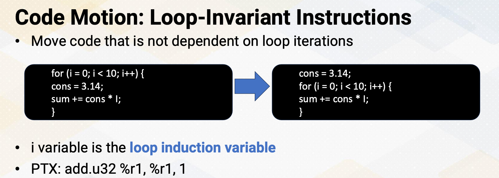
Code motion, specifically, the technique of moving loop-invariant instructions, involves relocating code that does not depend on loop iterations outside of the loop. This can potentially reduce the number of dynamic instructions. In this example, the cons variable receives a value of 3.14 every single loop iteration in the left side of the code. By moving this assignment outside of the loop, the statement can be executed only once. Here I also want to point out that the i variable in the loop is commonly referred as a loop induction variable. It is used to control the number of iterations and typically increment and decrement with each iteration of the loop. Loop induction variables can often trigger other compiler optimizations, which is one of the main reasons why we want to detect this loop induction variable. A common pattern of PTX code for the loop induction variable is add.u32 r1, r1, 1.
In this video, we have reviewed loop unrolling, function inlining, and strength reduction, which offer various optimization opportunities. We also saw the simple examples of these cases. And moving loop-invariant instruction is an example of code motion.
Module 11 Lesson 4 : Divergence Analysis
Learning Objective
- Describe static code analysis techniques to detect warp divergence
In this video we’ll show an example of one of the static GPU code analysis techniques, divergence analysis. The learning objective of this video is to describe static code analysis techniques to detect warp divergence.
Review: Divergent Branches
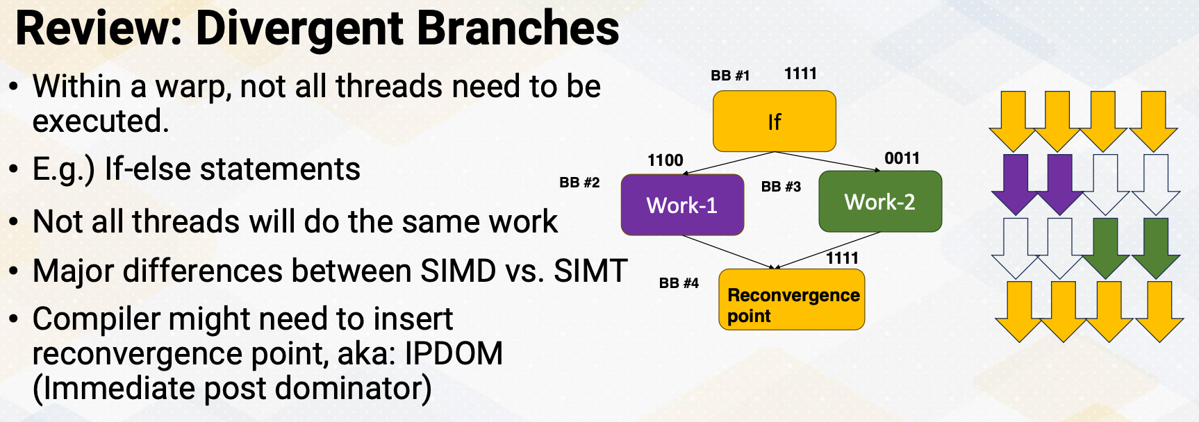
Just to review divergent branches means within a warp, now all threads will execute the same code. We have already studied how the hardware support divergent branches using SIMT stack. Since handling divergent branches might require compiler’s support, identifying divergent branch is important at compile time. In some cases, the compiler has to insert reconvergence point which is also known as immediate post dominator in the compiler’s term at static time. So the code example shows if else statement, and some thread goes to Work 1 and some thread goes to Work 2 and then the reconvergence point which is basic block 4 might need to be indicated by the compiler. So the compiler needs to know whether this if branch might be a divergent branch or not.
Divergence Analysis and Vectorization
Interestingly, divergent analysis has even longer history than GPUs. Converting loops into vector code, which is also called vectorization is the compiler’s job. In order to perform vectorization, it is also necessary to check whether all instructions within a loop will execute in a lock-step. Even a loop also has a branch, if all instructions within the branch execute the same way, then the code inside the branch can be also vectorized. So the compiler algorithm has even evolved to detect divergence. And GPUs also inherited those traditional vectorization tests to detect divergences. When there is a simple if else statement, these tests are relatively easy. When complex control flow graphs are combined with synchronization, then this test gets complicated.
Divergent Branches: Thread Dependency
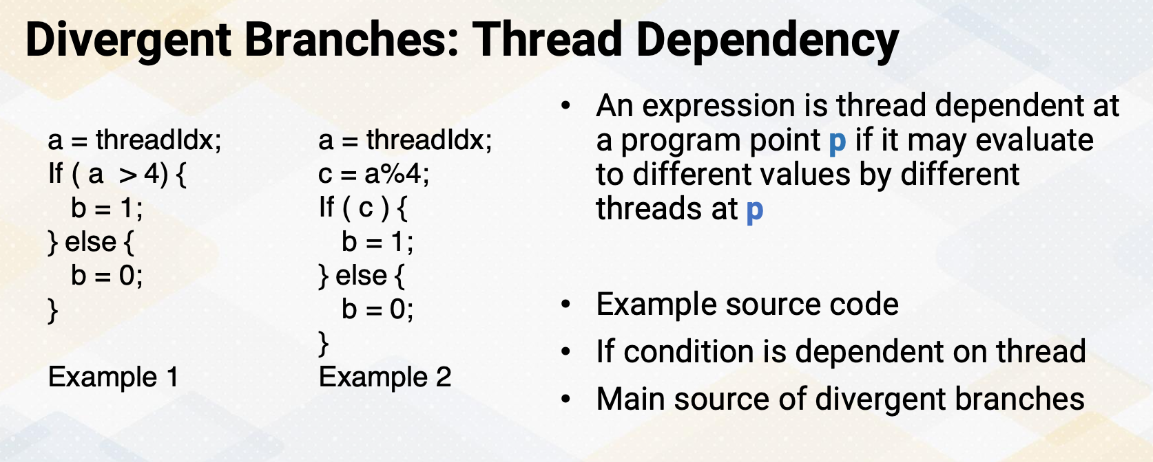
In the GPU code, if a branch condition is dependent on the thread ids, it will be a divergent branch. The more formal way of saying it is, in a program point p, if it is dependent on thread, it may evaluate to different values by different threads at p. Here are examples of source code. In this example, a is a threadIdx. The first example, the condition of if is directly dependent on a and the second example, c is dependent on a and conditional branch is dependent on c. In both cases, essentially the conditional branches are dependent on thread Ids. So this branch can be divergent branches.
How to Check Thread Dependency?
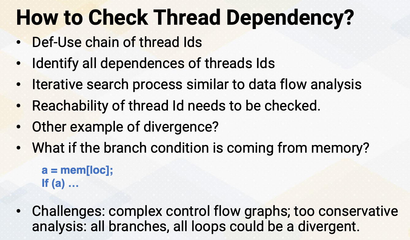
Then how to check thread dependencies? We can construct def-use chain of thread Ids. There are similar techniques that we have studied using data flow analysis. This is simply checking whether a branch condition is dependent on thread Ids and thread Id definitions can be reached over to the branch conditions. So this also requires iterative searching process that we have seen in other data flow analysis. So we identify all the branch conditions that are dependent on thread Ids. You might also wonder, are there any other example of divergent branches which are not dependent on thread Ids? For example, what if the branch condition is coming from the memory, a equals memory location, and if branch condition is dependent on a. If the location variable is constant across all thread, then a value will be also constant across all thread, so the branch won’t be divergent. But if the location variable is varied by thread Ids, then a value will be also changed. But in order to loop case of variable be dependent on thread Ids, they are essentially coming from thread Ids. so in general, if a branch, if they’re dependent on thread Id, they will be divergent. Divergent analysis requires thread Id checks and it ends up inserting reconvergence point information and some other additional information. Very conservative analysis might indicate too many branches as divergent branches. For example, all loops could be divergent. So the compiler algorithms need to trim down the conditions that are non divergent and this might get even more complicated if the control flow graphs are complex.
So in summary, we reviewed the conditions of work divergent check techniques. When the branches depend on thread Ids that becomes a divergent branches. This is an example of using the data flow analysis for GPU programming analysis.
Module 12: ML Accelerations On GPUs
Objectives
- Be able to understand the basic kernels of ML accelerators for GPUs
Required Readings:
- https://resources.nvidia.com/en-us-tensor-core Optional Readings:
- https://docs.nvidia.com/deeplearning/performance/dl-performance-matrix-multiplication/index.html
- https://images.nvidia.com/aem-dam/en-zz/Solutions/data-center/nvidia-ampere-architecture-whitepaper.pdf
Module 12 Lesson 1 : GPU and ML
Learning Objectives
- Explain the basic operations of machine learning workloads
- Describe the benefits of GPU for ML workloads
Hello. In this model, we’ll study how GPUs are used to accelerate ML applications. This video will help to understand the basic operations of machine learning workloads and describe the benefits of GPU for ML workloads.
Why are GPUs Good for ML?
So why are GPUs good for ML? Because many ML workloads have many floating-point operations, and they are highly data parallel operations. And GPUs are good for handling many parallel data because GPUs have many floating point operation units. So essentially, most of transistors inside the GPUs are used for providing floating-point operations. Furthermore, GPUs have high memory bandwidth memory systems. Although providing high memory bandwidth is coming from the memory technology itself, because GPU chips and memories are directly connected, which makes it easy for GPUs to employ high bandwidth memory chips such as HBM. And also, GPUs can easily employ flexible data formats such as tensor format, brain floating point format, integer 4 etc. Also, ML workloads are statistical computings. It works well with the GPU’s underlying execution models. For example, GPUs use weak memory consistency model and do not provide precise exceptions. Supporting those might require more hardware resource, but because GPUs do not require to support them, which goes well with ML statistical computing models.
DNN Operation Categories
In DNN operations, we can say that there are three major operations.
- Elementwise operations, as an example, activation operations.
- Reduction operations as examples are pooling maximum operations.
- Also has dot-product operations commonly used in convolution operations or GEMM.
And all these DNN operations are highly data parallel.
Background of GEMM
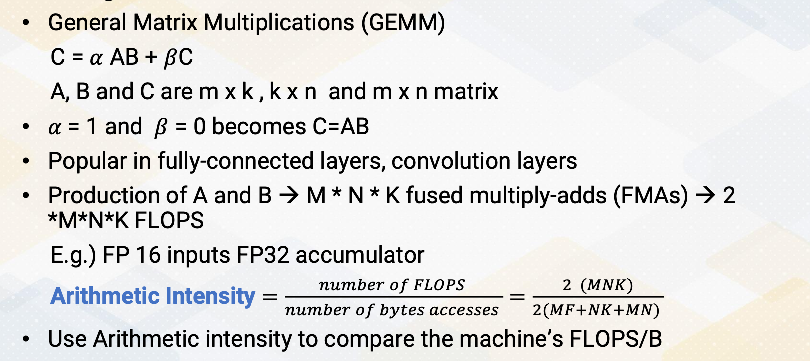
One of the most common operations, the GEMM, which is general matrix multiplication, can be represented as C equals alpha AB plus beta C. A, B, and C are m times k, k times n, and m times n matrix. Alpha beta are constants and they can even become zero. So alpha equals one and beta equals zero becomes C equals A times B. These GEMM operations are popular in fully connected layers or convolution layers. Let’s also think about arithmetic intensity.
In the GEMM operation. If we do a production of A and B, that requires M times N times K fused, multiply-adds, and one fused multiply-add includes two FLOPS. So total number of floating-points operations will be 2 times MNK. And if you assume, 16 bit of floating-point, although the accumulator is operated 32 bit, the number of bytes that each matrix data needs to bring will be 2 times MK+ NK+MN. Two is included because floating point 16 bit format requires to bring two bytes. Once you know the matrix sizes, you can compute this arithmetic intensity. Then you can compare whether the GPU machines can provide this arithmetic intensity. Although this assumption or this computation is based on the assumption that all these floating-point operation input values are coming from memory, which could have been also optimized by original caches, this gives the first order of approximations. Also, you can also use this arithmetic intensity to estimate if you optimize the memory data, what would be the arithmetic intensity and whether the GPU can support it or not.
Difference Between SIMD vs. Tensor
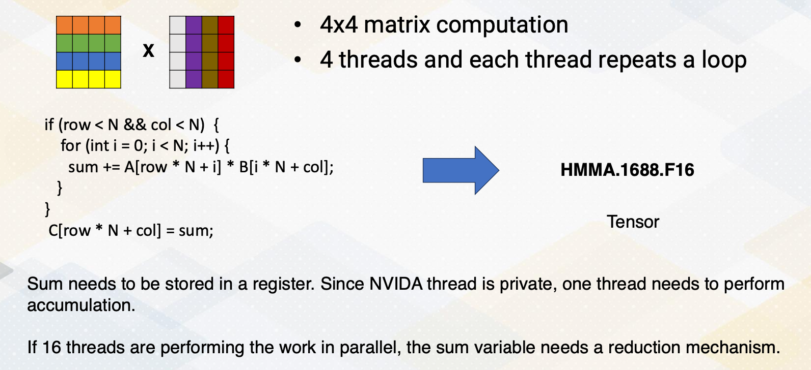
GPUs already provide SIMD operations, but GPUs also provide accelerator, which is also called tensor core for matrix multiplications. Let’s consider four by four matrix operations. To perform these four by four matrix multiplications, typically four threads are used and each thread repeats a loop, which is shown in this code. Because sum needs to be stored in a register, and since NVIDIA thread is private, one thread needs to perform these accumulations. So that requires the four loops within one thread. Four different threads can be performed in parallel, but these loops are executed in sequencer. Although, 16 threads could perform the work in parallel. In that case that some variable needs be accumulated in a different method such as using a shared memory, so that which might cause even more overhead. All these codes could be simplified if using a tensor core. Just simply say HMMA.1688.F16. That just simply says this is performing four by four matrix computations with 16 bit floating-point operations. This illustrates the difference between SIMD operations and tensor core operations.
SIMD/SIMT Operations of Matrix Multiplications
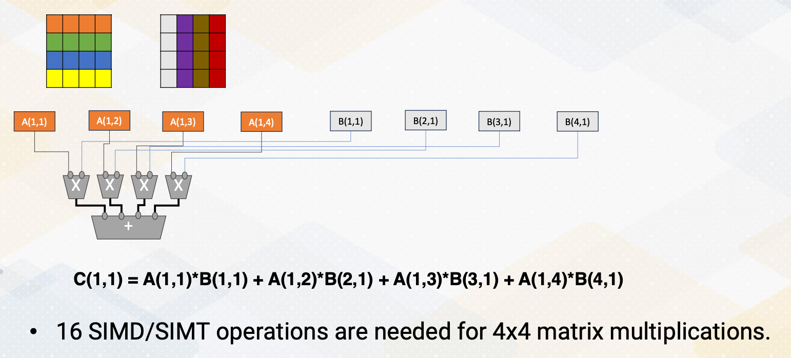
Although we could parallelize by having multiple operations, A and B in parallel. So they can compute this one element in sequence or in parallel. But that’s essentially what the tensor operations are doing it. If we’re using a SIMT operations, 16 SIMT or SIMD operations are needed to perform four by four matrix multiplications.
Tensor Cores
In tensor cores, it performs matrix multiply and accumulator calculations. And hundreds of tensor cores operating in parallel in one NVIDIA GPU, which enables massive increases in throughput and efficiency. To improve the performance even more, the sparsities are provided. As an example, A100 tensor core can execute 256 of FP 16 FMA operations. To improve the performance more, INT8 and INT4 or binary 1- bit predictions are added.
Matrix Multiplications with Systolic Arrays
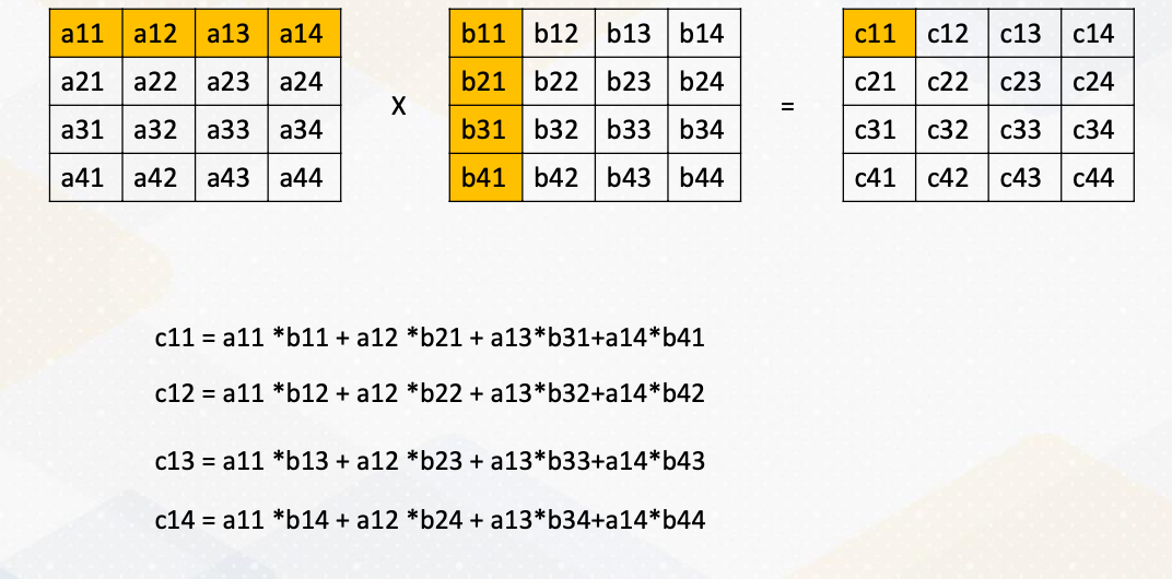
Traditionally, matrix multiplications or accelerate with the systolic arrays. Here it shows the matrix multiplications and it spell out each of these output. And just to illustrate, only the c12 are shown here.
Systolic Arrays Operations
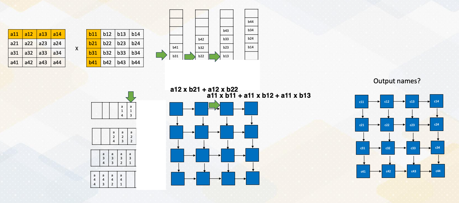
Then let’s consider how these operations can be performed in the systolic arrays. The basic idea of systolic arrays is data is moving across all these elements. Each of these blue box is performing matrix multiply and accumulation operations. First now to trying to fill out this input. The first rows are filled out here and this is second row and third rows and fourth rows. And this is storing these columns. And then each cycle one element or the element within these positions are feeding to here. And at the same cycle all these elements in these positions feed into here. So you can see that first elements will be computed from this a11 and b11, but these other positions are empty, which means the value will not be feed into this systolic array. At cycle 1, a11 times b11. B11 will be feedind here, a11 will be feeding here. And this blue box performs a11 times b11. In cycle 2, a11 value will be moved to the next element and b11 will be moved to this again, the next element. And the sum will stay here as a partial sum. Each of the blue arrays keeps storing the partial sums. So since now in this moment b12 is coming from here and a11 was coming from here will be performed the operations. The values was previous performed, a11*b11 is stored, and new value a12 times b21 will be performed and then added here. So each cycle, the a moves as row-wise and the b will move from the column wise. So in each cycle, they will receive the new values based on these positions. At the fourth cycles, we received all those elements we received the values. And each of these elements are performing the operations, that this one is performing the c11s, and this one performs c12, c13 and c14s. So this shows this output array format At the fourth cycles, all these elements are fully populated and it will take towards seven cycles to finish these operations. And here it shows the final outcomes.
Transformer Engine
New NVIDIA architecture also introduced a transformer engine which was introduced in the GH architecture. This was to accelerate the transfer layers. Transformer engine dynamically scales tensor data into representative range, which can also accelerate the performance. Furthermore, it supports FP8 operations. But one of the most important part of the transformer engine’s characteristic is it brings a chunk of data efficiently to fully utilize the tensor units. So moving the data is so much critical as the computer operates so high to keep up with this tensor cores. They also use TMA to generate addresses using a copy descriptor.
In summary, GPU accelerates matrix multiplications in ML workload. The SIMD and SIMT accelerate matrix multiplications, but dedicated matrix multiplication units improve the performance even more. And with all these accelerators, fully utilizing memory bandwidth is so critical.
Module 12 Lesson 2 : Floating Point Formats
Learning Objectives
- Describe IEEE Floating-point formats
- Explain the benefits of quantization
In this video, we’ll discuss floating point format. We’ll describe IEEE floating point format and we will also explain the benefits of quantization.
FP 16 vs. FP 32
FP16 versus FP32. FP16 uses the half precision of FP32, and IEEE standards have 32 bits for single precision and 64 bit for double precisions. In traditional scientific computations, floating points are used to provide much high precision values such as single or double precisions.
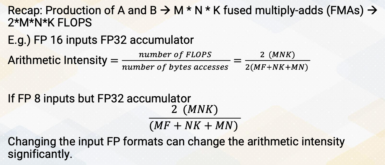
But with the ML workload, now we’re reducing the precisions. The reason is, if you think about arithmetic intensities, if you keep these accumulators the same, the number of floating point operations are the same, but number of bytes that needs to be bring can be changed significantly depending on what kind of floating point format we are using. So instead of FP16, if you use FP8, then even though the number of FLOPs are the same, number of bytes that needs to be accesses can be reduced by half, therefore, the arithematic intensity will be increased by double. So this is an easy way of changing the input format and also changing arithmetic intensity significantly. So this is an easy way of changing the arithmetic intensity by simply changing the input floating point format.
Benefits of Quantization
What are the benefits of quantization? It reduce the storage size, it increase arithmetic intensity, and the newer floating point excution units also increase the throughput if we reduce the floating point precisions. And ideally, if you perform FP8, then this might be 2x performance of just doing FP16 by considering the number of bits. This was the case in the earlier time of floating point operations. The quantizations that reduced input sizes, but the number of floating points operation per cycle will remain the same. But newer ML workloads, newer ML accelerators, as we reduce the floating point operation size, the throughputs also increased.
Floating Point Basics
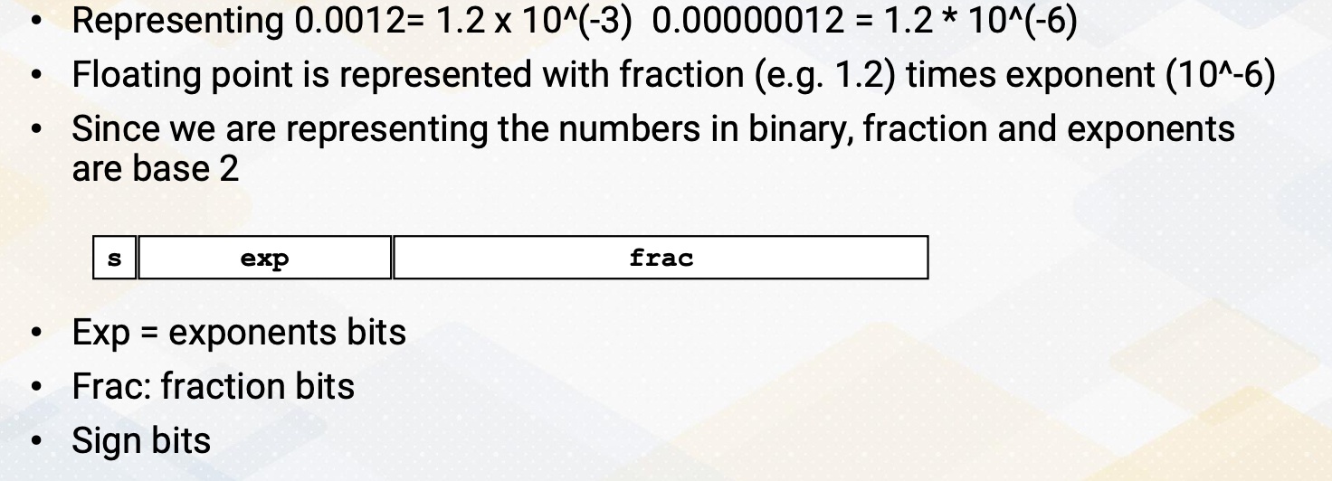
Let’s just review the floating point basis. Let’s say, we want to represent value 0.0012. This could have been represented by 1.2 times 10^-3. Similarly, 0.000012 will be 1.2 times10^-6. Floating point is represented with a fraction, 1.2 times exponent. In both case, fraction values are the same, only the exponent values are different. Since we are representing the numbers in binary, fraction and exponents are based on 2. So simple floating point format will be sign bit, exponent bit, and fraction bit.
Different Floating Point Formats
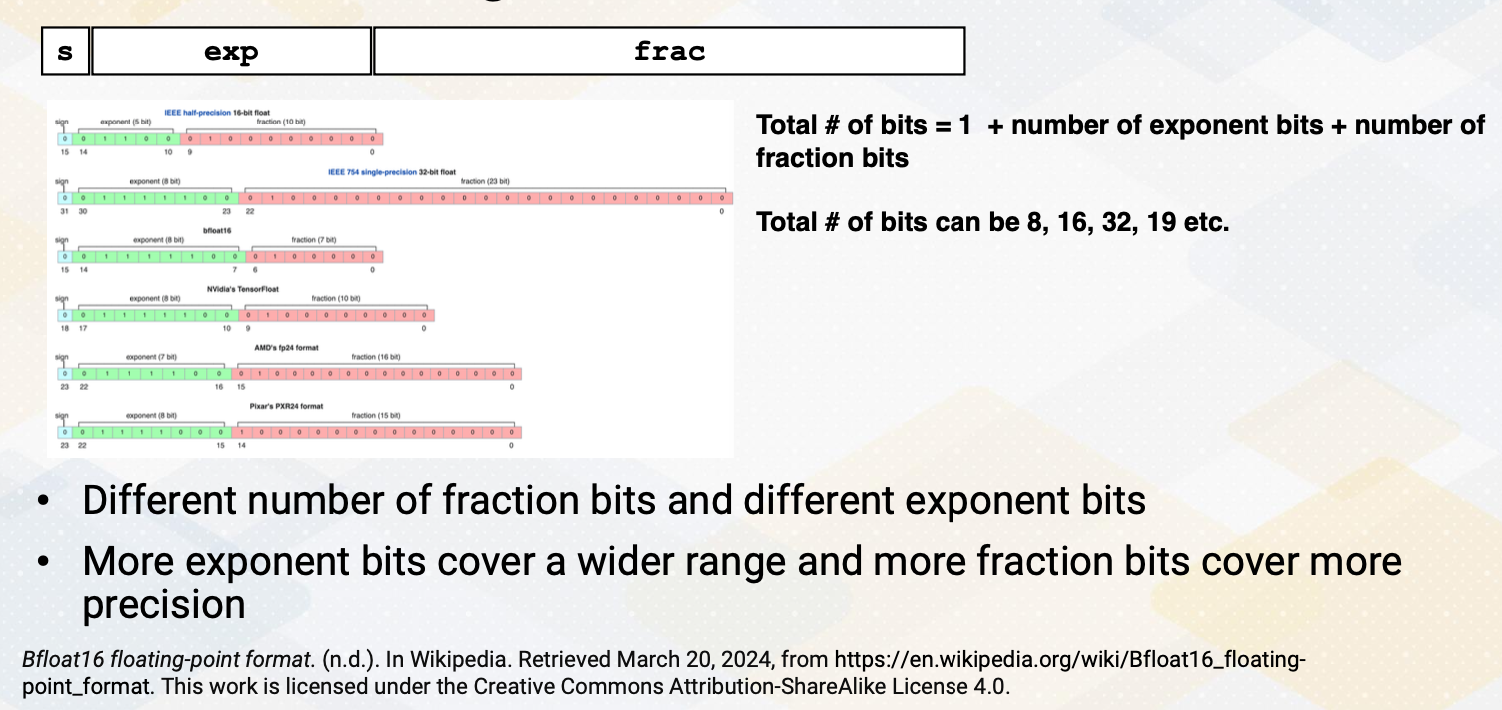
And there are several different floating point formats. The total number bit is 1 for sign bit, plus number of exponent bit plus number of fraction bit. By reducing total number bits, then we can reduce the total data size. So there are a lot of emphasis of reducing total number bits. There can be 8, 16, 32 or it can be some odd number such as 19. Now within this total sum, it could also have different number of bits for fraction and different number of bits for exponent. Typically, more exponent bit cover a wide range of values, and more fraction bit covers more precisions.
Some More Details
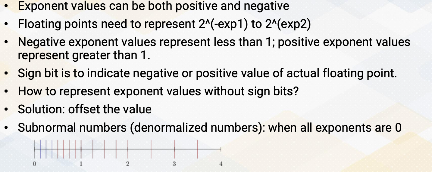
And there are some more details regarding the floating point operations. First, exponent values can be both positive and negative. Because floating point needs to be represented to 2 to the exponent, and exponent can be negative number or positive number, then negative exponent represent a value less than 1 and positive exponent represent value greater than 1. The sign bit that represent floating point format actually means the actual floating point value is sign bit. So in order to indicate exponent values are negative or positive, the IEEE standard used offset to indicate the values. And then there are other more complications such as representing subnormal values or denormalized values when all exponents are zero.
Floating Point Number Representations
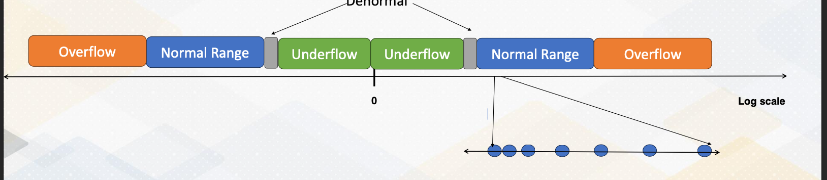
This diagram illustrates the floating point of value representations. There is a value, and very close to zero are on the flow that cannot be represented. To increase the value that can represent the bar close to 0, we use denormalized values, which will be indicated by gray colors. And then there is a huge normal range, since the figure is shown at low scale, the normal range is much bigger. And then after the end of the normal range, there’s overflow. But if you’re also zooming the normal range, the values that are close to zero are much more fine grain represented, And as it goes more close to overflow regions, the values loose precisions.
IEEE 754 Formats
So IEEE 754 formats indicate how you represent sign, exponent, and fraction or mantissa bit. And there are also special values, positive and negative zero, positive and negative input values and narrow numbers, and also represented the denormalized values. And also rounding modes such as round up and round down.
Quantization
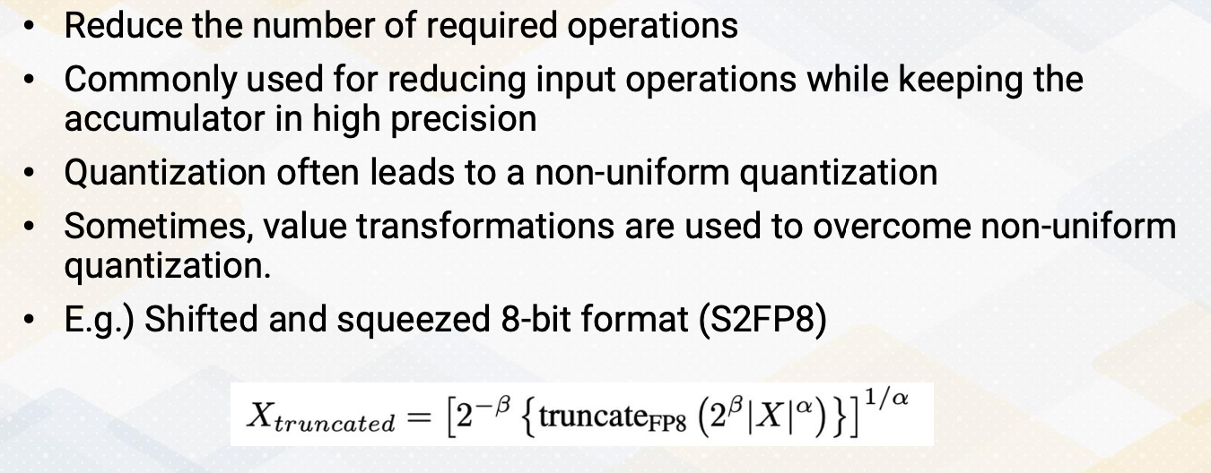
So quantization reduce number of bits that also reduce number of required operations. It’s commonly used for reducing the input operations while keeping the accumulator in high precisions. And quantizations often leads to a non-uniform quantization. Sometimes the value transformations are used to overcome this non-uniform quantization. One of the example is shifted and squeezed 8-bit format that uses the following transformation equations to convert the values. Such transformations are needed to provide more high precision value that close to zero, because the values that are close to zeros are much more valuable in ML workload. In summary, quantizations can improve the estimate intensity and also reduce data movement cost by reducing the storage size. And quantization can also improve the efficiency of computations.
Module 12 Lesson 3 : Tensor Core
Learning Objectives
- Describe the architecture design methods for ML accelerator components on GPUs
- Explain the main design criteria
In this video, we’ll discuss how to design ML accelerators on GPUs. The learning objectives of the video are to describe the architecture design method for ML accelerator components on GPUs. We will also discuss the main design criteria.
Designing ML Accelerator Units on GPUs
Let’s sit back and think about how to design ML accelerators on GPUs. We want to consider the following factors. What functionalities we want to design and what benefit we’ll get over the existing GPUs by having a dedicated accelerator. How we want to design the compute units, and how many of them we want to add. What would be the data storage and movement to send the data to these accelerators.
Common Steps of Designing Accelerators
The common steps of design accelerators will be, first, we want to identify frequently executed operations. This can be done by understanding the algorithm or by doing a profiling.
Second, we want to understand the performance benefit because the underlying architecture already have highly data parallel execution unit, so we need to understand how much performance benefit we’ll get by having a dedicated accelerator. Using the existing GPU memes software approaches, using the existing ISAs, and hardware approaches can simplify some of the operations with research from the hardware.
When you add more hardware, that means we have to design the interface and how to program those new hardware. What ISA to add and how we feed the data into the accelerator? What storage format we’re going to use. We’re going to use registers and memories as private shared registers.
After that, we also want to consider whether we want to combine multiple accelerator component into one component. Typically, by having multiple features in the one hardware improve the programmabilities and usabilities, but that comes with overhead of more hardware and might even incur timing overhead. So this design decision needs to be done very carefully.
Matrix Multiplication Accumulator
GPUs chose to use matrix multiplication accumulator as additional hardware component because these operations are mostly commonly used in ML workload. Although SIMD operations are good, but it still requires row by row operations. If we use a larger matrix multiplication unit, this could have been implemented with the systolic arrays. So here are the design decisions, do you want to have a many small matrix multiplication units or do we want to have a larger matrix multiplication unit? We also need to consider area and programmability choices. As we dedicate more area to the matrix multiplication unit, we lose the hardware resource that can be used for other GPU operations. NVIDIA started with the 4 by4 matrix multiplication unit. Matrix multiplication accelerators are also commonly used in other architecture such as Intel and R. And Intel’s AMX, advanced matrix extensions, support 16*16 matrixes.
Possible Matrix Multiplication Unit Design
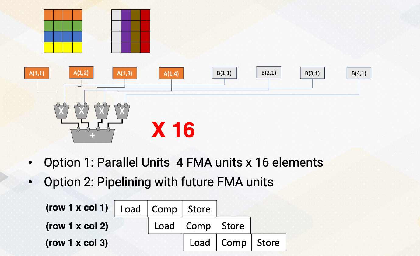
How do you design the matrix multiplication unit? We could go for the systolic arrays, but you can see in the previous video, systolic array requires filling time and draining time. With a smaller matrix multiplication unit such as filling and draining time might be wasteful, so we might want to consider other options. One of the option is, we can just have many parallel units, the matrix multiplications that which performs one role in one column, and we can have 16 of them to support matrix multiplication unit.
Another option can be using a pipeline method that you share the same hardware, and first it performs first row times first column, and the next cycle it performs first row and second column, and so on. Each of this operation requires load and compute and store times. By doing a pipeline, we can improve the throughput. So this is a trade-off. In terms of throughput-wise, we could have a mini parallel unit or we could have the multiple pipelining of PMM unit.
Data Storage and Movement
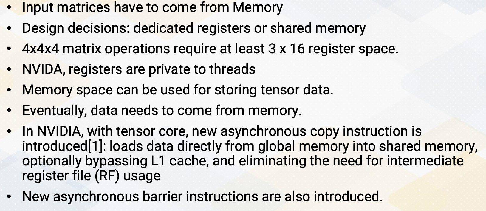
Another important factor to consider is, what kind of format do you want to use, and how do you send the data to this matrix multiplication unit? Because input matrix have to come from the memory, a few design decisions need to be made. Do you want to have dedicated registers or use shared memory? 4 by 4 by 4 matrix operations require any 3 times16 register space. And NVIDIA’s registers are private thread makes even more complicated design choices. So it could use memory space to store the tensor data, but this memory space close the tensor unit, and the original matrix will be stored in the global memory. So it is required to send a lot of data from the global memory to the memory space that are closed the matrix multiplication unit. Hence in NVIDIA, the new asynchronous copy instructions are introduced that loads data directly from the global memory into the shared memory. And optionally bypassing L1 cache and eliminating the need for intermediate register file usages. They also introduce asynchronous barrier instructions along with these asynchronous copy instructions.
Supporting Sparse Operations
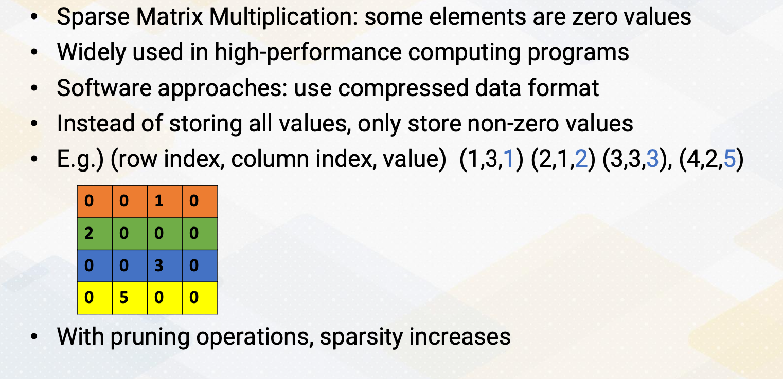
So NVIDIA GPU architecture also supports sparsity operations to improve the performance. In general, sparse matrix multiplications are the matrix operation that some elements are zero values which are widely used in high performance computing programs, especially graph workload. Software approaches use the compress data format instead of storing all the values, only storing non-zero values. In the following matrix, for 4 by 4 matrix, instead of storing all the 0, 0, 1, 0, etc, we could just store row index value, column index value, and the value of this matrix, for example, 1,3,1 2,1,2, etc. By having so, we can just have only four element, but there are overhead of storing these index values. There are several sparse value storage format that even further simplify the row index values or column index values to compress it.
Supporting Sparsity in Hardware
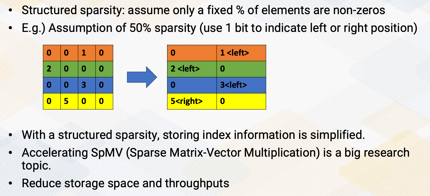
With the ML algorithms pruning operations, this sparsity increases and supporting sparsity operations becomes very critical. When it’s supporting sparsity operations in hardware, it is critical to support structured sparsity to simplify the hardware. Structured sparsity means, it assumes a certain percent of the elements are non-zeros. For example, if you assume the 50% sparsities, then this 4 by 4 element, the 16 element can be represented with only eight element, because we assume 50% of sparsities. And this compressed data also needs to have an index bit, but it can be simplified with one bit to indicate whether the compressed values coming from the left side of these columns or right side of the columns. The first two 0,0 becomes just 0, second 1, 0 becomes 1, and we need to indicate this 1 comes from the left side of the column. 2,0 becomes 2, and 0,0 becomes 0, etc, 0,0,0, and three zeros. And 0, 5, the 5 is coming from right side that column, so we need to indicate this 5 is coming from the right-side columns. So with structured sparsity, storing index information becomes very simplified. And also, building hardware becomes much more simpler by just assuming this fixed sparsities. Accelerating this SpMV, sparse matrix-vector multiplication is a big research topic that actively going on. Supporting sparsity reduces storage space and also improves the throughput.
In this video, we reviewed the design trade-offs of design ML accelerators on GPUs and the steps. We also reviewed the GEMM and SPMV operations.